IC layout optimization to improve yield

a layout optimization and optimization technology, applied in the direction of cad circuit design, program control, instruments, etc., to achieve the effect of reducing critical area contribution cost, and further reducing critical area of layou

Inactive Publication Date: 2009-03-10
GLOBALFOUNDRIES INC
View PDF7 Cites 109 Cited by
  • Summary
  • Abstract
  • Description
  • Claims
  • Application Information

AI Technical Summary

Benefits of technology

[0006]The invention provides a method of optimizing a VLSI layout using critical area information, design methodology rules, manufacturing ground rules, manufacturing process data, and automation. Starting with an initial integrated circuit physical design, the invention associates variables with the positions of the edges of shapes in the design. The invention determines the critical area contribution cost using the variables. Critical area contributions comprise a measure of electrical fault characteristics of the spacing between edges and represent the probability of a fault occurring during manufacturing. The invention optimizes the position and dimensions of the edges to reduce critical area contribution cost in an iterative method in a first direction across the integrated circuit design to produce a revised integrated circuit design. The invention optionally repeats this process with the revised integrated circuit design in a second direction to further reduce critical area contribution cost, and then optionally repeats the optimization in the first dimension and second dimension depending on whether the critical area of the layout can be further reduced.
[0007]Unlike existing yield optimization methods, the method of the present invention uses real manufacturing data to identify where possible failures will occur during the manufacturing process. Each failure type is given a weight according to the likelihood that it will adversely affect yield. This information is fed into the optimization algorithm. The method uses critical area analysis (CAA) techniques to identify critical areas in the design including Voronoi diagrams, common-run calculations, and Monte Carlo simulations. Other known algorithms such as genetic algorithms, neural networks, and statistical analysis methods could also be used. Once critical areas have been identified and weighted, the method alleviates the impact of the critical areas by using several techniques. For example, shape modification of a structure, and moving the location of structures within the design.
[0008]To minimize the use of available resources and speed the design process, the method focuses on higher weighted failures when more than one failure is possible in a given area and mitigates those critical area risks. The design optimization process eliminates the need for making a trade-off between alleviating critical failures and available design time and resources because it takes the same amount of time to fix all of the identified critical areas that have been identified from the manufacturing data.

Problems solved by technology

One model for yield estimation is based on the concept of critical area, which represents the main computational problem in the analysis of yield loss due to random (spot) defects during fabrication.

Method used


Image

  • IC layout optimization to improve yield
  • IC layout optimization to improve yield
  • IC layout optimization to improve yield

Examples


first embodiment

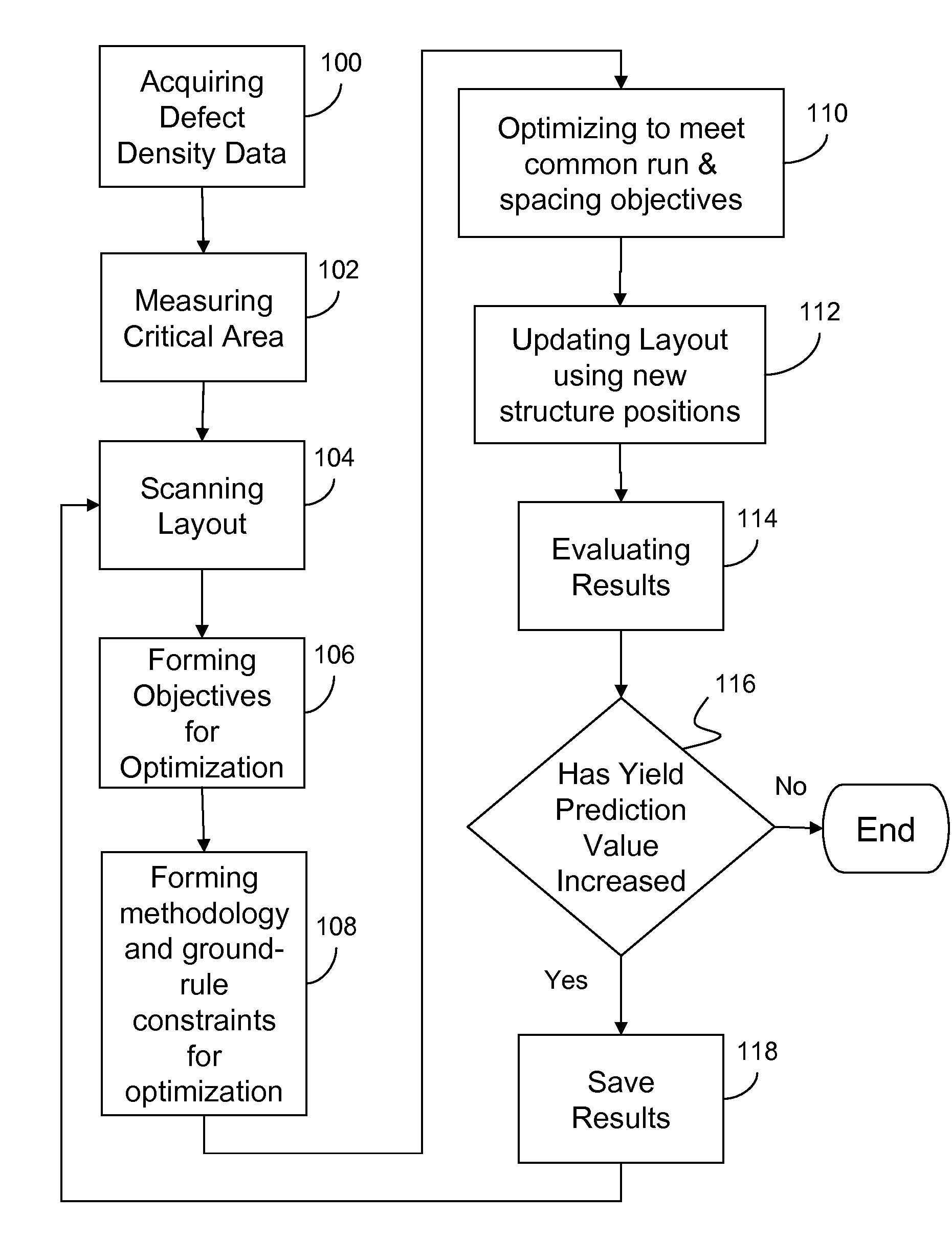
[0022]FIG. 1 illustrates the method of a first embodiment, which identifies critical area in an IC layout using common run. In step 100, the method acquires defect density data provided by the manufacturing process. This data gives the estimated fault density for various defect mechanisms (e.g., short-circuit-causing faults on layer M1) and provides the input for step 102. In step 102 the method measures critical area based on the defect data.

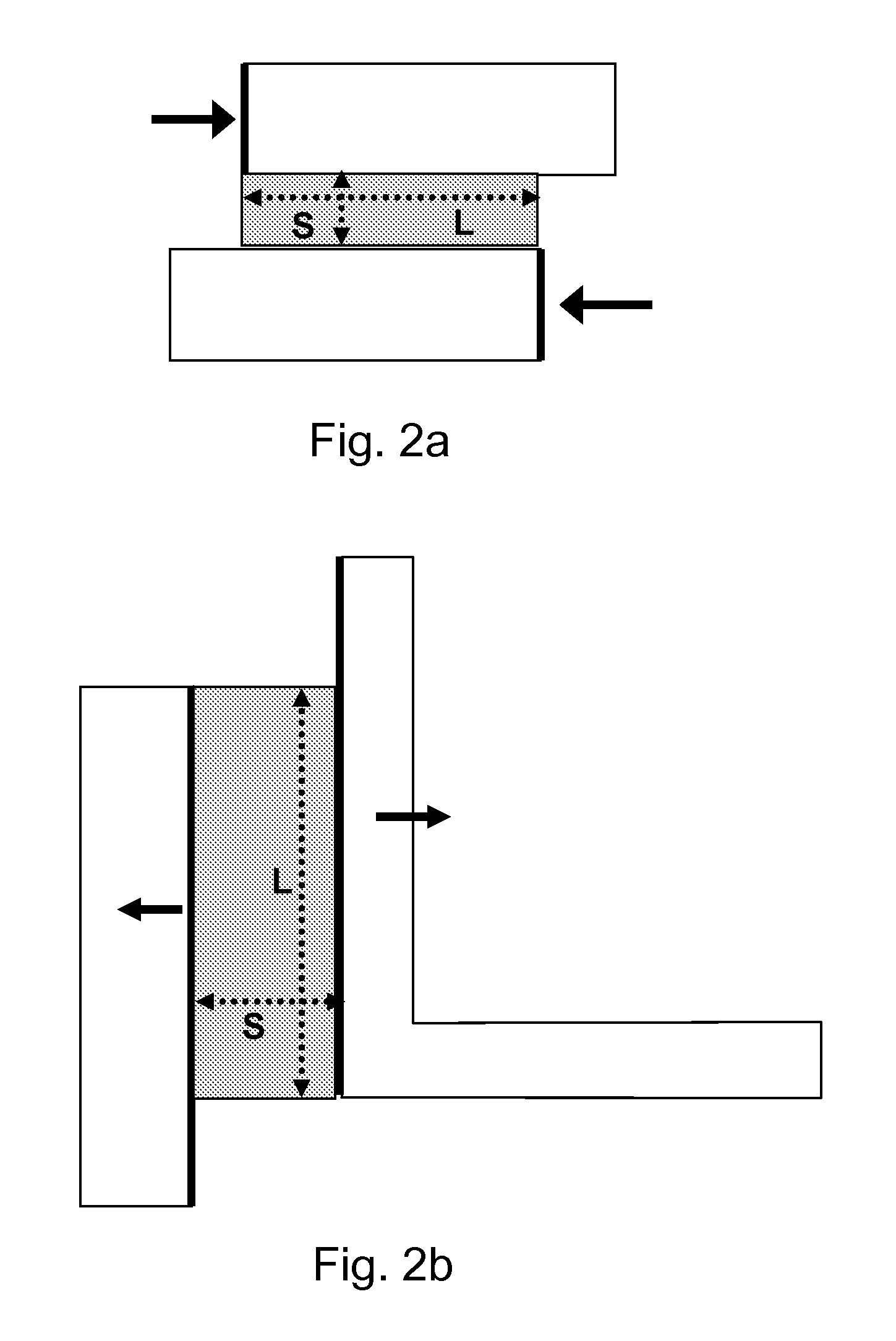
[0023]In step 104, for a given layout, the method scans the layout and records L / S for each shape in the design, where L is the common run between adjacent parallel edges and S is the distance between the edges. The method compares the recorded information to the defect density data to identify critical areas and further, identify the critical areas with the higher probability of failures. The weight assigned to each of these critical areas is the product of L / S and a layer-specific constant for shorts, opens, random defects, or combinations of...

second embodiment

[0050]In the present invention, the method of identifying critical area in a VLSI design uses Voronoi diagrams, an example of which is shown in FIG. 4. A Voronoi diagram is used to enhance the computation of critical area. A Voronoi diagram of a set of 2D geometric elements (polygons, line segments, points) is a partition of the plane into regions representing those points in the plane closest to a particular geometric element. Here, closest is defined in terms of an appropriate geometry to represent a defect. These regions are called Voronoi cells 310, each of which is associated with its defining geometric element 312, called the owner of the cell. The set of points which separates two Voronoi cells is called a Voronoi bisector 314. The point where three or more Voronoi bisectors 314 (or Voronoi cells 310) meet is called a Voronoi vertex 316.

[0051]Based on the circuit design and under an appropriate geometry, Voronoi diagrams can be constructed to model the effect of extra-materia...

third embodiment

[0065]FIG. 10 illustrates the method of the third embodiment, which identifies critical area in an IC layout using geographical area information and associated critical area values to those locations. In step 600, the method acquires defect density data provided by the manufacturing process. This data gives the estimated fault density for various defect mechanisms (e.g., short-circuit-causing faults on layer M1) and provides the input for step 602. In step 602 the method measures critical area based on the defect data.

[0066]In step 604, for a given layout, the method scans the layout and records critical area values for each geographical area in the design. The method compares the recorded information to the defect density data to identify and map critical areas.

[0067]In step 606, the method builds a set of pair-wise objectives in one direction (e.g. vertically, horizontally) called the optimization direction, within the critical areas identified in step 604. For each critical area ...


PUM


Abstract

A method of and service for optimizing an integrated circuit design to improve manufacturing yield. The invention uses manufacturing data and algorithms to identify areas with high probability of failures, i.e. critical areas. The invention further changes the layout of the circuit design to reduce critical area thereby reducing the probability of a fault occurring during manufacturing. Methods of identifying critical area include common run, geometry mapping, and Voronoi diagrams. Optimization includes but is not limited to incremental movement and adjustment of shape dimensions until optimization objectives are achieved and critical area is reduced.

Description

BACKGROUND OF THE INVENTION[0001]1. Field of the Invention[0002]The present invention relates to a method of optimizing VLSI circuit designs using manufacturing data and various algorithms to ensure better yields in IC manufacturing.[0003]2. Background of the Invention[0004]The critical area of a very large scale integration (VLSI) layout is a measure that reflects the sensitivity of the layout to random defects that are introduced during the manufacturing process. Critical area is widely used to predict the yield of a VLSI chip. Yield prediction is essential in today's VLSI manufacturing due to the growing need to control cost. One model for yield estimation is based on the concept of critical area, which represents the main computational problem in the analysis of yield loss due to random (spot) defects during fabrication. Spot defects are caused by particles such as dust and other contaminants in materials and equipment and are classified into two types: “extra material” defects ...

Claims


Application Information

Patent Timeline
Patent Type & Authority Patents(United States)
IPC IPC(8): G06F17/50
CPCG06F17/5068G06F30/39
Inventor ALLEN, ROBERT J.BAKER, FAYE D.CHU, ALBERT M.GRAY, MICHAEL S.HIBBELER, JASONMAYNARD, DANIEL N.TAN, MERVYN Y.WALKER, ROBERT F.
Owner GLOBALFOUNDRIES INC
Why Eureka
Try Eureka