Substrate processing system

a processing system and substrate technology, applied in the direction of conveyors, instruments, photosensitive materials, etc., can solve the problems of variability in the quality of the substrate, the inability of the carrier unit to carry another substrate in some cases, and the processing time difference between the substrates, so as to reduce the size of the substrate processing system, reduce the processing time difference, and flexiblely deal with

Inactive Publication Date: 2009-03-17
TOKYO ELECTRON LTD
View PDF4 Cites 2 Cited by
  • Summary
  • Abstract
  • Description
  • Claims
  • Application Information

AI Technical Summary

Benefits of technology

[0009]The present invention has been developed in consideration of the above points, and its object is to flexibly deal with various processing recipes for substrates, reduce the processing time difference among substrates and carriage waiting time of the substrates, and reduce the size of the substrate processing system without using a central carrier unit as in the prior art.
[0011]According to the present invention, since the first units can vertically move to be able to transfer the substrate between at least two first units arranged in the vertical direction and the second unit, a plurality of carriage routes of the substrates are formed between the first units and the second unit. Therefore, it is possible to carry the substrates between the units in various combinations and flexibly deal with various processing recipes for the substrates even without using a central carrier unit as in the prior art. Furthermore, since there is no central carrier unit as in the prior art, it is possible to reduce the processing time difference among the substrates and carriage waiting time of the substrates. Moreover, it is possible to reduce the size of the substrate processing system by a space corresponding to the eliminated central carrier unit.
[0013]Also in this case, a plurality of carriage routes of the substrates are formed between the first units and the second unit. Therefore, it is possible to carry the substrates between the units in various combinations and flexibly deal with various processing recipes for the substrates even without using a central carrier unit as in the prior art. Furthermore, it is possible to reduce the processing time difference among the substrates to reduce the variations in quality of the substrates. Further, the carriage waiting time of the substrates can be reduced to improve the throughput. It is possible to reduce the size of the substrate processing system by a space corresponding to the eliminated central carrier unit.

Problems solved by technology

According to the above-described substrate processing system, however, the one central carrier unit is used to carry many substrates, and therefore, during carriage of one substrate, the carrier unit cannot carry another substrate in some cases.
For this reason, it is difficult to carry out the substrate from the processing unit at an ideal timing at all times, thereby possibly increasing the periods of some substrates staying in the processing units to cause a processing time difference among the substrates.
For example, the thermal processing time difference greatly affects the processing result of the substrates and can cause variations in quality of the substrates.
Further, if the carriage waiting time of the substrate is increased, the time required for the whole processing of the substrate accordingly increases, and the increase can lead to a reduction in throughput.
Therefore, a relatively large space is required for the processing station, resulting in a large substrate processing system as a whole.

Method used


Image

  • Substrate processing system
  • Substrate processing system
  • Substrate processing system

Examples


Embodiment Construction

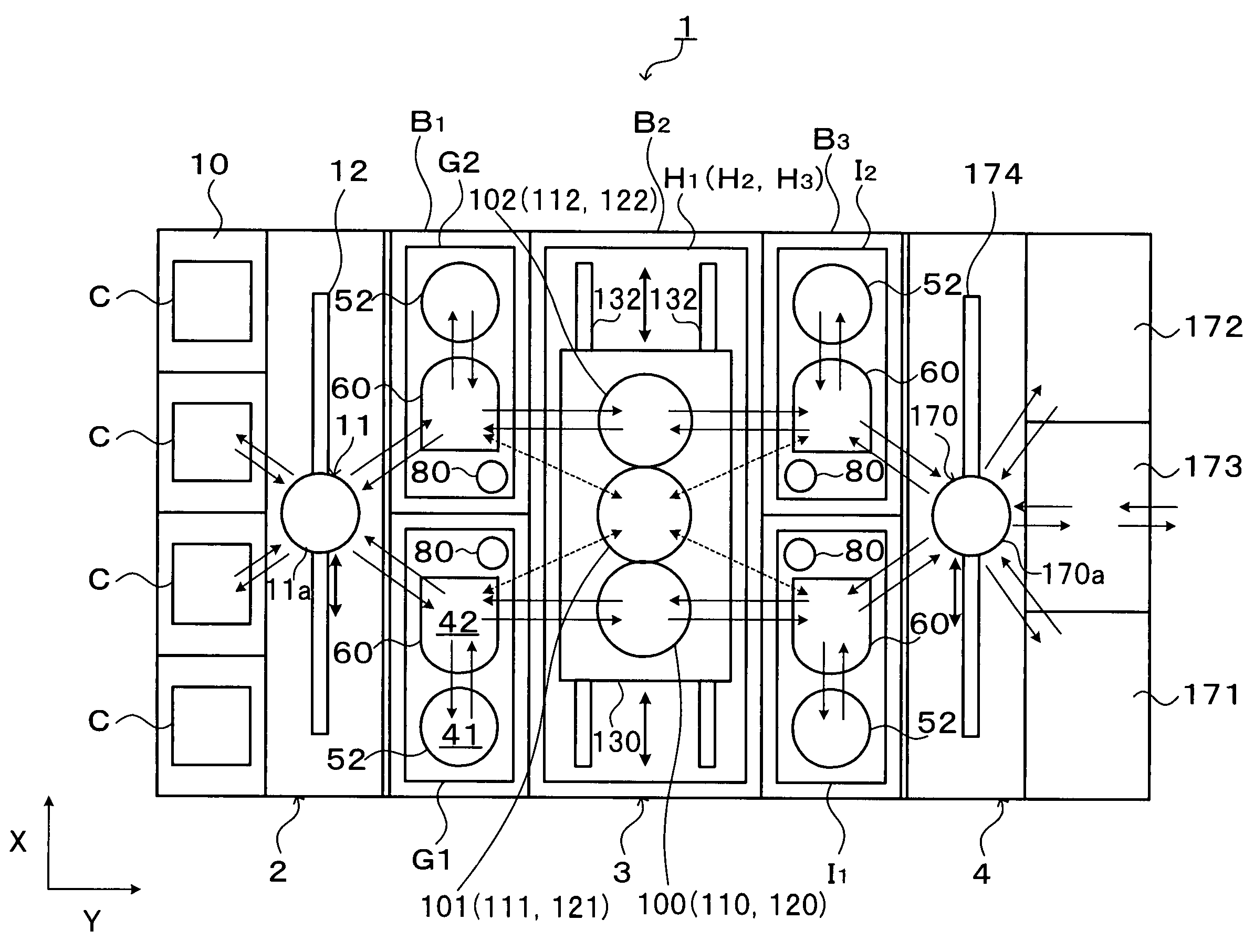
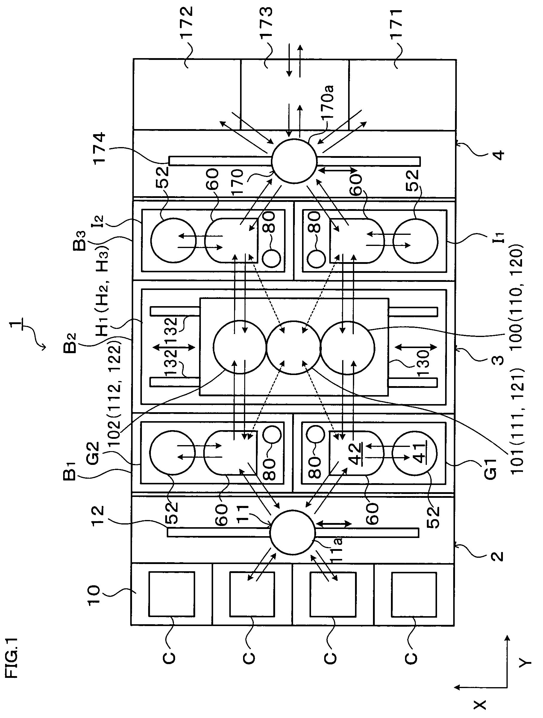
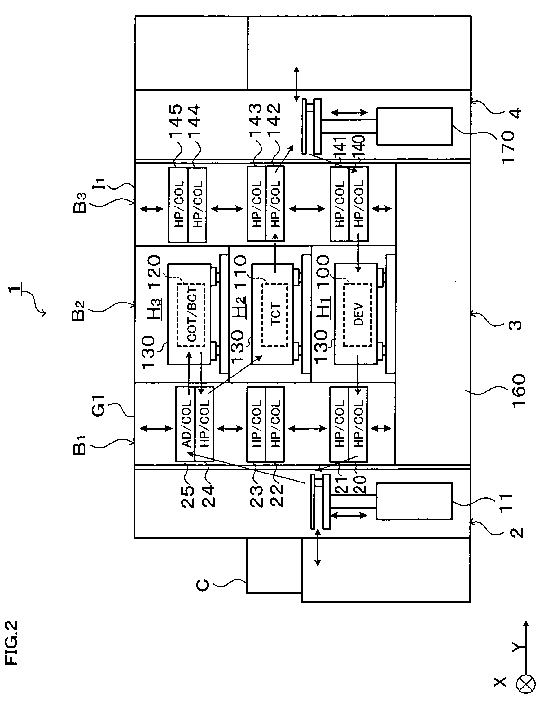
[0038]Hereinafter, a preferred embodiment of the present invention will be described. FIG. 1 is a plan view showing the outline of a configuration of a substrate processing system 1 according to this embodiment.

[0039]The substrate processing system 1 has, as shown in FIG. 1, a configuration in which, for example, a cassette station 2, as a carry-in section or a loader / unloader section, for carrying, for example, 25 wafers per cassette as a unit from / to the outside into / from the substrate processing system 1 and carrying the wafers W into / out of cassettes C; a processing station 3 provided adjacent to the cassette station 2 and including a plurality of units for performing various kinds of processing or treatments in the photolithography process; and an interface section 4 for transferring the wafers W to / from an aligner (not shown) provided adjacent to the processing station 3, are integrally connected together. The cassette station 2, the processing station 3, and the interface sec...


PUM

PropertyMeasurementUnit
processing timeaaaaaaaaaa
carriage waiting timeaaaaaaaaaa
sizeaaaaaaaaaa

Abstract

In the present invention, a plurality of first units capable of accommodating the substrate and a second unit are provided, in which a substrate is carried between the first unit and the second unit. The first units and the second unit are arranged side by side in a plan view, and at least one of the plurality of the first units is a processing unit for performing processing for the substrate. The plurality of first units are arranged in a line in the horizontal direction, and at least two first units adjacent to each other in the horizontal direction of the plurality of first units are movable in the horizontal direction to be able to transfer the substrate to / from the second unit. According to the present invention, the substrate processing system including a plurality of units flexibly deals with various substrate processing recipes and reduces the processing time difference among substrates and the carriage waiting time of the substrate.

Description

[0001]This application claims foreign priority based on Japanese patent applications No. 2005-157924, filed May 30, 2005, No. 2005-159069, filed May 31, 2005, and No. 2005-162951, filed Jun. 2, 2005, the contents of which are incorporated herein by reference in their entirety.BACKGROUND OF THE INVENTION[0002]1. Field of the Invention[0003]The present invention relates to a substrate processing system for performing processing for a substrate.[0004]2. Description of the Related Art[0005]Conventionally, processing for a substrate, for example, a semiconductor wafer or the like often includes a plurality of processes, and the processing is continuously performed using a plurality of processing units. Accordingly, the substrate processing is typically performed in a substrate processing system in which a plurality of processing units are collectively installed.[0006]For example, a substrate processing system for performing the photolithography process includes a loader / unloader section ...

Claims


Application Information

Patent Timeline
Patent Type & Authority Patents(United States)
IPC IPC(8): G03D5/00B65G35/00
CPCH01L21/67173H01L21/67178H01L21/67742H01L21/67745H01L21/67161H01L21/6719H01L21/67196H01L21/67754
Inventor KIYOTA, KENJI
Owner TOKYO ELECTRON LTD
Why Eureka
Try Eureka