Single-atom tip and preparation method thereof

a single atom tip and preparation method technology, applied in the manufacture of electrode systems, cold cathode manufacturing, electric discharge tube/lamp manufacture, etc., can solve the problems of complex conventional preparation of single atom tip, poor yield rate, and need to be operated under ultra-high vacuum. , to achieve the effect of simplifying the method

Active Publication Date: 2009-03-24
ACAD SINIC
View PDF17 Cites 31 Cited by
  • Summary
  • Abstract
  • Description
  • Claims
  • Application Information

AI Technical Summary

Benefits of technology

[0009]The objective of this invention is to provide a simplified method for the preparation of single atom tips.
[0010]Another objective of this invention is to provide a low-cost preparation of single atom tips.

Problems solved by technology

Although the single atom tip is very useful, it is difficult to prepare a single atom tip for commercial applications.
Although the above-mentioned methods could successfully produce a single atom tip, they need to be operated under ultra-high vacuum environment.
The conventional preparation of the single atom tip is complicated and with poor yield rates.
The single atom tip so prepared does not have a thermodynamically stable structure either, thus the operation lifetime is short and regeneration of single atom tips is very difficult or impossible.
The metal tips so prepared don't have a well-defined structure of atoms at their apex and applications of such metal tips outside the ultra-high vacuum system are not possible.
These drawbacks hinder the single atom tip from commercial applications.
This is not convenient for most applications of single-atom tips.

Method used


Image

  • Single-atom tip and preparation method thereof
  • Single-atom tip and preparation method thereof
  • Single-atom tip and preparation method thereof

Examples


embodiment i

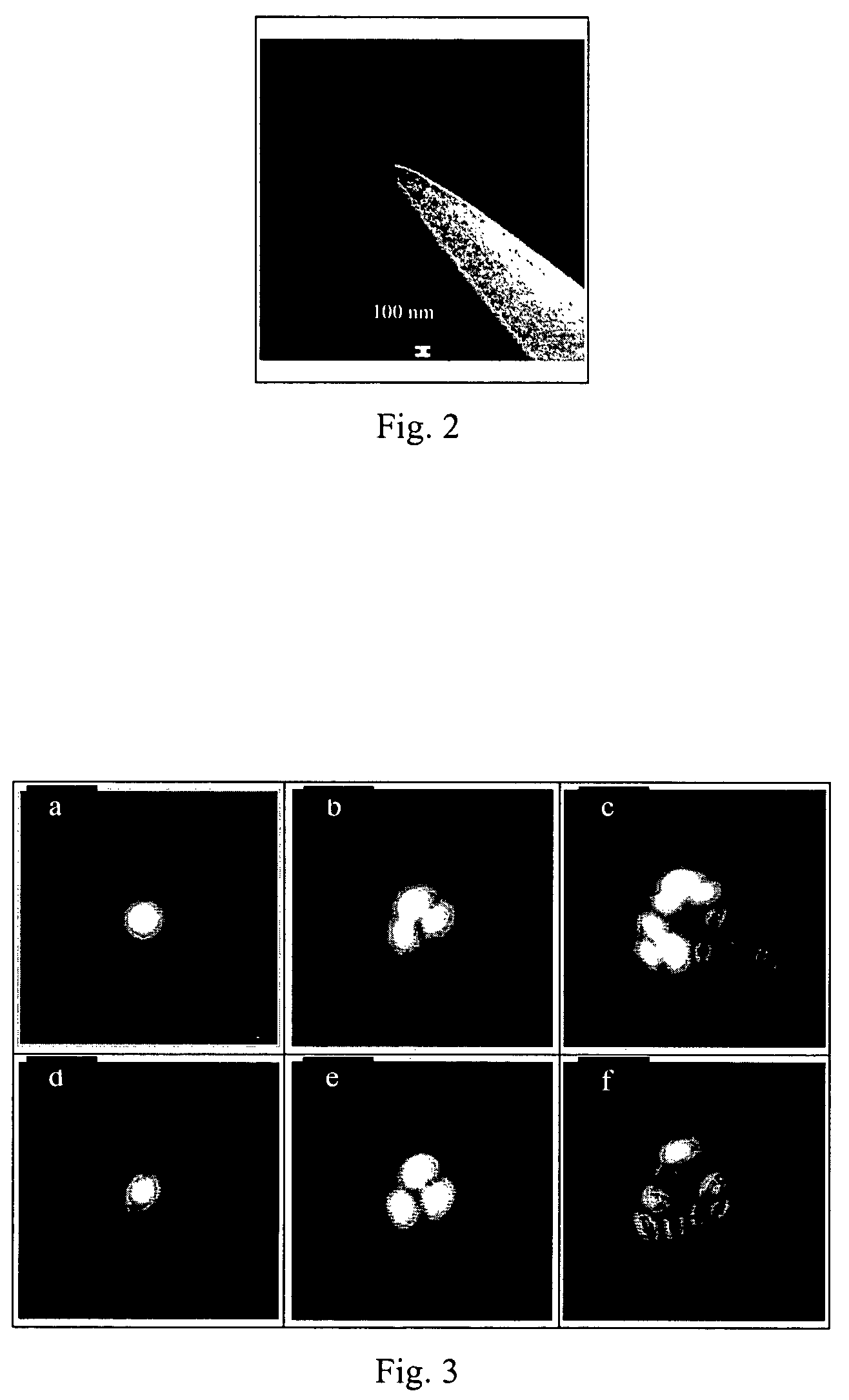
[0040]Etching: A tungsten single crystal wire is electrochemically etched into a tungsten tip. The metal tip is cleansed in water. The apex of the etched metal tip, as well as its size, is shown in FIG. 2.

[0041]Shielding: The metal tip is shielded with nail polish as shielding layer, at areas other than the apex, such that only the apex of the metal tip is exposed.

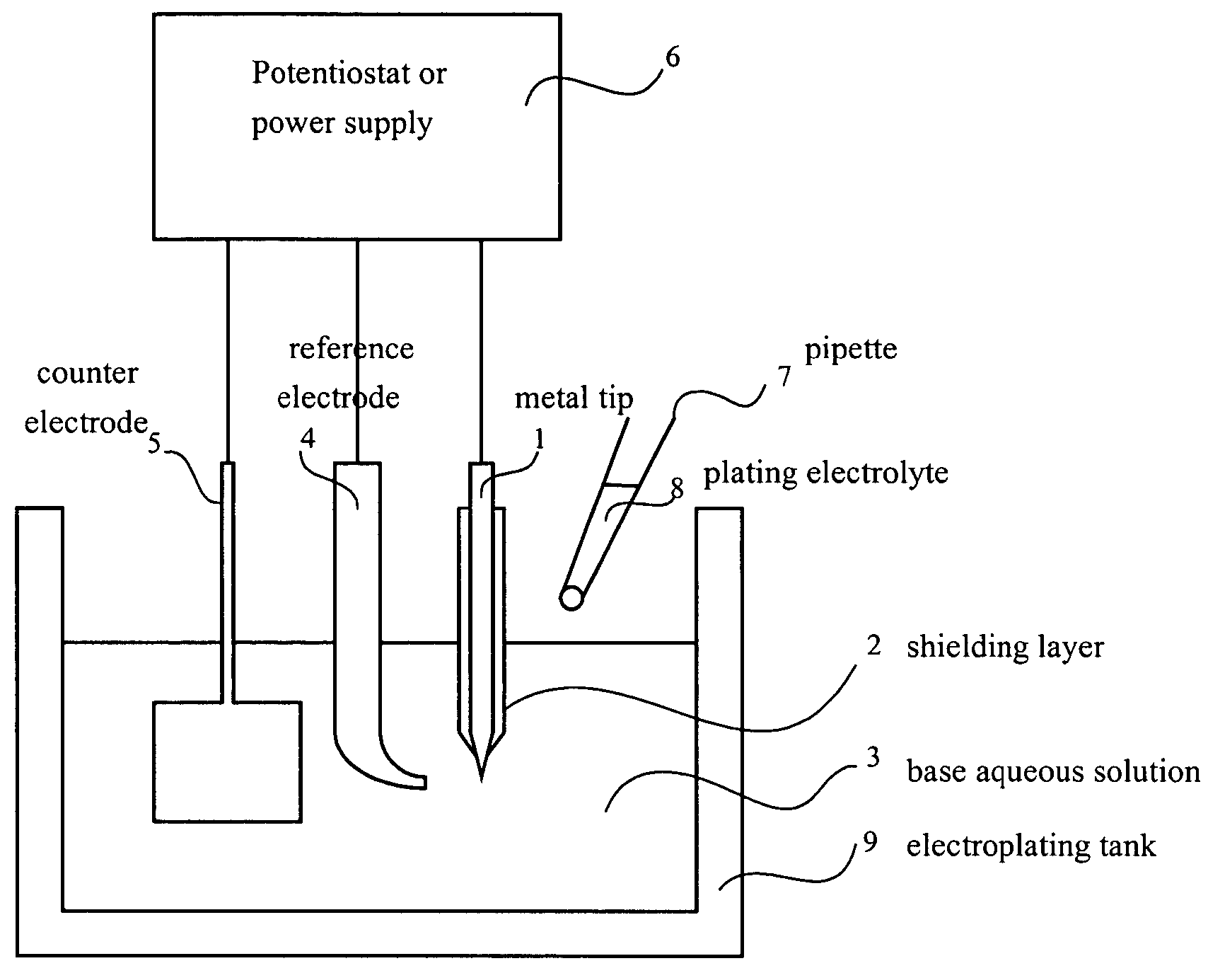
[0042]Electrochemical system: In the system as shown in FIG. 1, the metal tip is immersed into the base aqueous solution. A saturated calomel electrode (SCE) is used as reference electrode, platinum electrode as counter electrode, and an EG&G 366A potentiostat as power supply. Proper quantity of palladium electrolyte in the pipette is prepared.

[0043]Cathodic cleaning: When the metal tip is positioned in the base aqueous solution (0.1M HCl), −0.6V (vs. SCE) is applied to cathodic process the metal tip for 10 minutes.

[0044]Plating: Drop the palladium-plating electrolyte (0.1 mM PdCl2+0.1M HCl) into the base aqueous solution...

embodiment ii

[0050]In an electrochemical system same as that of Embodiment I, tungsten tip is plated and annealed according to the same process of Embodiment I, except that the shielding of the metal tip is omitted and that the tungsten tip is plated in a concentration of palladium ion of 3×10⁻⁷M with −0.6V (vs. SCE) for 15 seconds. The plated metal tip is further annealed in vacuum chamber at 700□ for 20 minutes and then at 500□ for over 17 hours, followed by annealing at 700□ for 5 min. An atomic level facet pyramid structure on W (111) surface is observed, as shown in FIG. 4.

[0051]In comparison to Embodiment I, in Embodiment II the concentration of the palladium electrolyte is increased and the shielding process is omitted, so that more palladium is plated to the tungsten tip. In addition, the annealing temperature is lowered and the annealing time is extended so that possible range of conditions in forming the pyramid structure may be realized. As shown in FIG. 4a, the topmost layer of the p...

embodiment iii

[0052]In an electrochemical system as Embodiment I, a metal tip is plated and annealed according to the same process of Embodiment I, except that the plated metal tip is first sunk into the base aqueous solution to be electrochemically annealed under +0.4V (vs. SCE) for 15 minutes and the shielding nail polish is then removed with acetone before it is annealed in the vacuum chamber under 700□ for 5 minutes. The finished metal tip is observed and a facet atomic level pyramid structure on the W (111) surface is found, as shown in FIGS. 5a and 5b.

[0053]If compared with Embodiment I, in Embodiment III an electrochemical annealing process is added to shorten its anneal time in the vacuum chamber. FIG. 5a shows that the topmost layer of the apex has only one atom, meaning that the metal tip so prepared is a single atom tip. When the topmost atom is evaporated, 3 atoms in the second layer are observed, as shown in FIG. 5b. Thus, it is shown that the same pyramid structure is formed at the...


PUM

PropertyMeasurementUnit
negative voltageaaaaaaaaaa
negative currentaaaaaaaaaa
anodic potentialsaaaaaaaaaa

Abstract

This invention discloses an electrochemical method for the preparation of single atom tips to replace the traditional vacuum evaporation method. The invented method for preparation of single atom tips includes the following steps: A substrate single crystal metal wire etched electrochemically to form a tip. The surface of the metal tip is cleaned. A small quantity of noble metal is plated on the apex of the tip in low concentration noble metal electrolyte. Annealing in vacuum or in inert gas ambient to diffuse the additional electroplated noble metal atoms and thus a single atom tip is formed on the surface of the substrate. The present invention also discloses the single atom tip so prepared. The single atom tip of this invention has only a very small number of atoms, usually only one atom, at its apex.

Description

FIELD OF INVENTION[0001]The present invention relates to method of preparation of single-atom tip, especially to electrochemical method of preparation of single-atom tip and the single-atom tip so prepared.BACKGROUND OF INVENTION[0002]The single-atom tip, with its special geometric shape and physical features, may be used as key component for advanced scientific equipments, such as scanning probe microscopy, field-emission electron microscopy, electron holography, electron energy spectroscopy, electron diffraction or interferometer, electron lithography, ion gun, low-energy electron microscopy etc. It may also be used in commercial electronic products such as flat panel display.[0003]The term “single-atom tip” pertains to a metal tip, ending with one atom at its apex. Because there is only one atom at the apex, the single-atom tip is an ideal scanning probe. Take the scanning tunneling microscope (STM) as an example. In order to realize optimal spatial and spectral resolution, the p...

Claims


Application Information

Patent Timeline
Patent Type & Authority Patents(United States)
IPC IPC(8): C25D5/34G01Q10/00G01Q70/16
CPCB82Y35/00C25D5/022C25D5/38C25D5/48C25D5/50C25F1/00G01Q70/16C25D5/003H01J9/025H01J37/073H01J37/08Y10T29/49002C25D3/50H01J2237/06341H01J2237/0807C25D3/48
Inventor HWANG, ING-SHOUHKUO, HONG-SHITSONG, TIEN T.FU, TSU-YI
Owner ACAD SINIC
Why Eureka
Try Eureka