Method of forming solder connection portions, method of forming wiring substrate and method of producing semiconductor device

a technology of wiring substrate and solder connection, which is applied in the direction of soldering apparatus, manufacturing tools, non-printed masks, etc., can solve the problems of increasing the cost of producing semiconductor devices and mounting substrates, becoming difficult to form solder bumps relying on diameter differences, and achieving favorable and reliable production

Active Publication Date: 2009-03-24
SHINKO ELECTRIC IND CO LTD
View PDF8 Cites 18 Cited by
  • Summary
  • Abstract
  • Description
  • Claims
  • Application Information

AI Technical Summary

Benefits of technology

[0010]Concretely, embodiments of the present invention provide the method of forming solder connection portions of different diameters on the electrode pads favorably and reliably, the method of forming a wiring substrate by using the method of forming the solder connection portions and the method of producing a semiconductor device by using the method of forming the solder connection portions.
[0021]In this case, the solder balls placed on the first electrode pads or on the second electrode pads are held by the base mask, and are suppressed from deviating, enabling the solder connection portions to exhibit the effect of improved reliability.

Problems solved by technology

When the solder bumps have different diameters as described above, however, it becomes difficult to form the solder bumps relying, for example, upon the printing method if the pitches become narrow.
When the collected solder balls other than the placed solder balls are to be used again, therefore, it becomes difficult to sort them out relying on a difference in the diameters.
This causes an increase in the cost of producing the semiconductor devices and the mounting substrates.
According to the method taught in the patent document 2, further, when the solder balls to be placed have a small difference in the diameters (sizes), it is probable that solder balls may be placed on different (wrong) opening portions (electrode pads) arousing a problem from the standpoint of mounting precision.
If it is attempted to simultaneously mount the solder balls of different sizes on a mask as in a related art (e.g., patent document 2), a problem arouses in that solder balls of different diameters are also made present.
When the solder balls other than those solder balls that are placed are to be used again, therefore, it becomes difficult to sort out the solder balls depending upon the diameters.

Method used


Image

  • Method of forming solder connection portions, method of forming wiring substrate and method of producing semiconductor device
  • Method of forming solder connection portions, method of forming wiring substrate and method of producing semiconductor device
  • Method of forming solder connection portions, method of forming wiring substrate and method of producing semiconductor device

Examples


first example

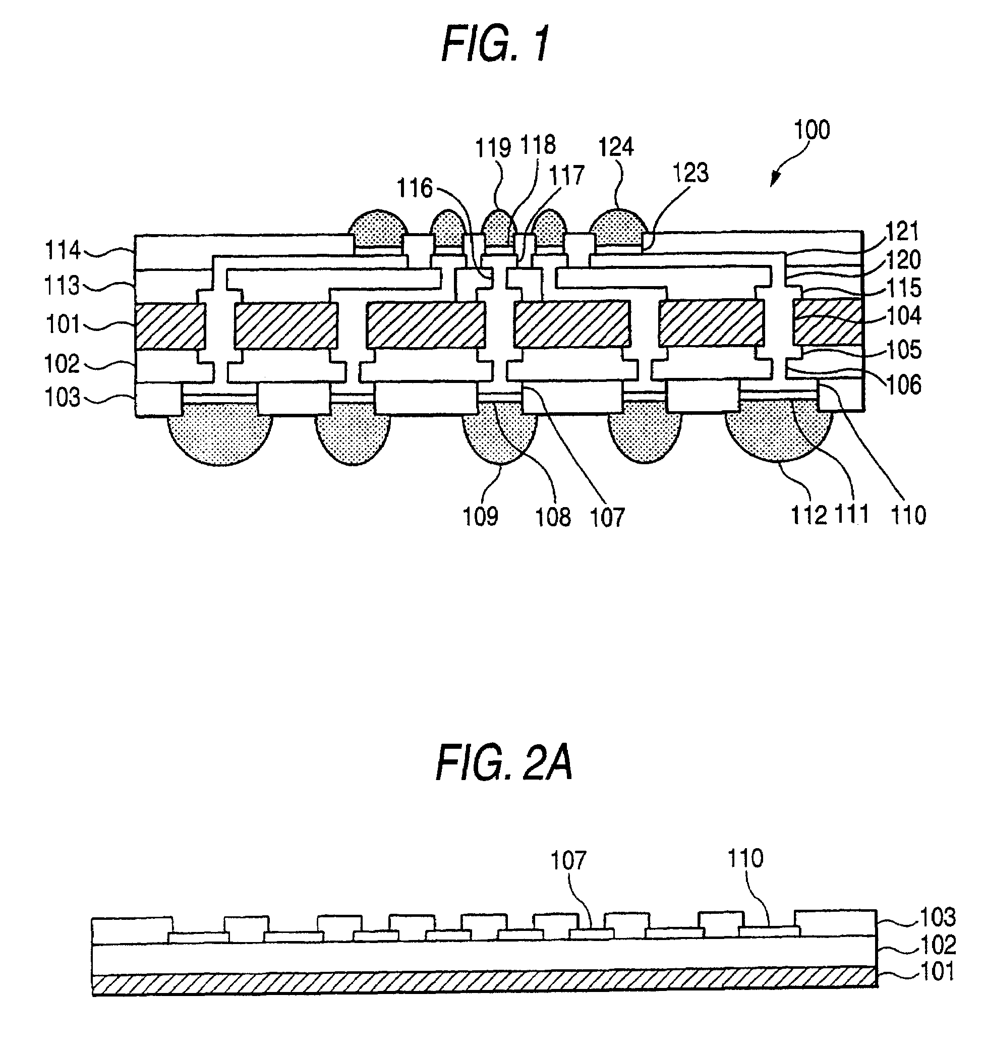
[0039]FIG. 1 is a sectional view schematically illustrating the structure of a wiring substrate produced by the method (described later) of forming solder connection portions according to a first embodiment of the invention.

[0040]Referring to FIG. 1, a wiring substrate (mounting substrate) 100 has a core substrate 101 made of, for example, a prepreg member, and a plurality of via-plugs 104 so as to penetrate through the core substrate 101.

[0041]Pattern wirings 105 connected to the via-plugs 104 are formed on a first surface of the core substrate 101, and pattern wirings 115 connected to via-plugs 104 are similarly formed on a second surface of the core substrate on the side opposite to the first surface.

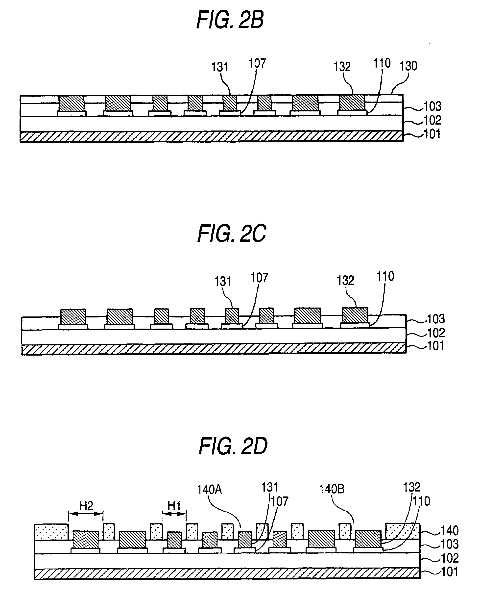
[0042]Further, an insulating layer 102 is formed so as to cover the pattern wirings 105, and via-plugs 106 are formed in the insulating layer 102 so as to be connected to the pattern wirings 105. Moreover, electrode pads 107, 110 connected to the via-plugs 106 are formed on the insul...

second embodiment

[0071]FIG. 3 is a sectional view schematically illustrating a semiconductor device 200 formed by the method of producing a semiconductor device according to a second embodiment of the invention.

[0072]Referring to FIG. 3, the semiconductor device 200 includes a semiconductor chip 201 having electrode pads 203, 205 formed by a known method. A solder resist layer 202 is formed surrounding the electrode pads 203 and 205. Solder connection portions (solder bumps) 204, 206 are formed on the electrode pads 203 and 205, the solder connection potions (solder bumps) 204, 206 being formed by the method of forming solder connection portions of the first or second embodiment.

[0073]The solder connection portions 204, 206 are formed by the method illustrated in the first embodiment (FIGS. 2A to 2K).

[0074]In this case, the electrode pads 203 correspond to the electrode pads 107, and the electrode pads 205 correspond to the electrode pads 110. Further, the solder connection portions 204 correspond t...

third embodiment

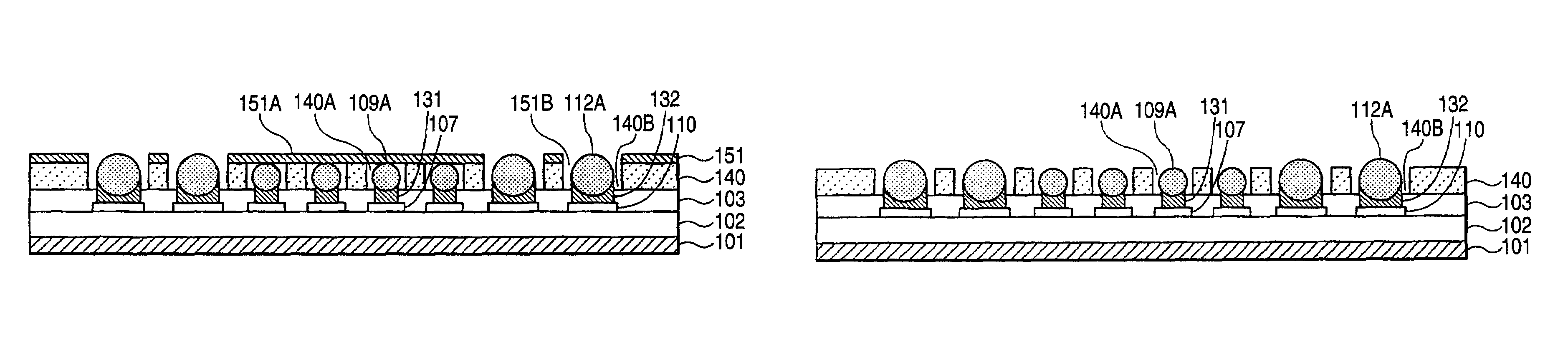
[0076]FIG. 4 is a view of a semiconductor device 300 obtained by flip-chip-mounting the semiconductor device (semiconductor chip) 200 described in the second embodiment on the wiring substrate 100 described in the first embodiment. A semiconductor device can be thus formed by mounting the semiconductor device (semiconductor chip) having a plurality of solder connection portions of different sizes on the wiring substrate having a plurality of solder connection portions of different sizes. Further, when the semiconductor device 200 is mounted in the above structure, the solder connection portions (solder bumps) may be formed on both the wiring substrate 100 side and the semiconductor device 200 side, or may be formed on either side only.


PUM

PropertyMeasurementUnit
sizeaaaaaaaaaa
diameteraaaaaaaaaa
sizesaaaaaaaaaa

Abstract

A method of forming solder connection portions on first electrode pads and on second electrode pads, comprises a first step of arranging solder balls on the first electrode pads by arranging a first mask on a base mask; a second step of arranging solder balls on the second electrode pads by arranging a second mask on the base mask; and a third step of melting the solder balls. The base mask has first opening portions corresponding to the first electrode pads and second opening portions corresponding to the second electrode pads and having a size different from that of the first opening portions. The first mask has opening portions corresponding to the first opening portions and covering the second opening portions. The second mask has opening portions corresponding to the second opening portions and covers the first opening portions.

Description

[0001]This application claims priority to Japanese Patent Application No. 2006-108878, filed Apr. 11, 2006, in the Japanese Patent Office. The priority application is incorporated by reference in its entirety.TECHNICAL FIELD[0002]The present disclosure relates to a method of forming solder connection portions, a method of forming a wiring substrate by using the method of forming the solder connection portions and a method of producing a semiconductor device by using the method of forming the solder connection portions.RELATED ART[0003]Efforts have been made to highly densely integrate connection portions (electrode pads) of semiconductor chips accompanying the modern trend toward highly densely mounting the semiconductor chips. Therefore, the semiconductor chips have been mounted by using solder connection portions which are so-called solder bumps (salient electrodes) in order to highly densely arrange the connection portions of the semiconductor chips.[0004]According to the above m...

Claims


Application Information

Patent Timeline
Patent Type & Authority Patents(United States)
IPC IPC(8): H01L23/488
CPCB23K3/0623H01L21/4853H01L23/49816H01L23/49838H01L24/17H05K3/3478H01L24/14Y10T29/49222H01L2224/13099H01L2224/16225H01L2924/01029H01L2924/01046H01L2924/01079H01L2924/15311H05K3/3436H05K3/3452H05K3/3489H05K2201/094H05K2201/10674H05K2203/041H05K2203/043H05K2203/0485H05K2203/0557H05K2203/0574H05K2203/1476H01L2924/01006H01L2924/01019H01L2924/01033H01L2924/014Y10T29/49144Y10T29/49149B23K2201/42B23K2101/42H01L2224/05571H01L2224/05573H01L2924/00014H01L2224/05599
Inventor SAKAGUCHI, HIDEAKIHIGASHI, MITSUTOSHI
Owner SHINKO ELECTRIC IND CO LTD
Why Eureka
Try Eureka