Method for fabricating storage node contact in semiconductor device

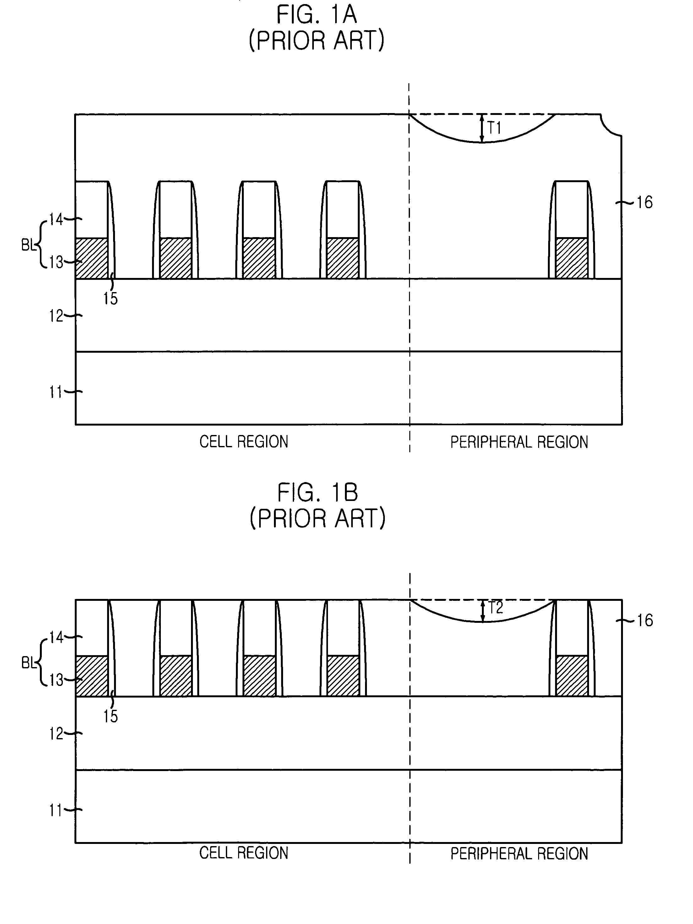
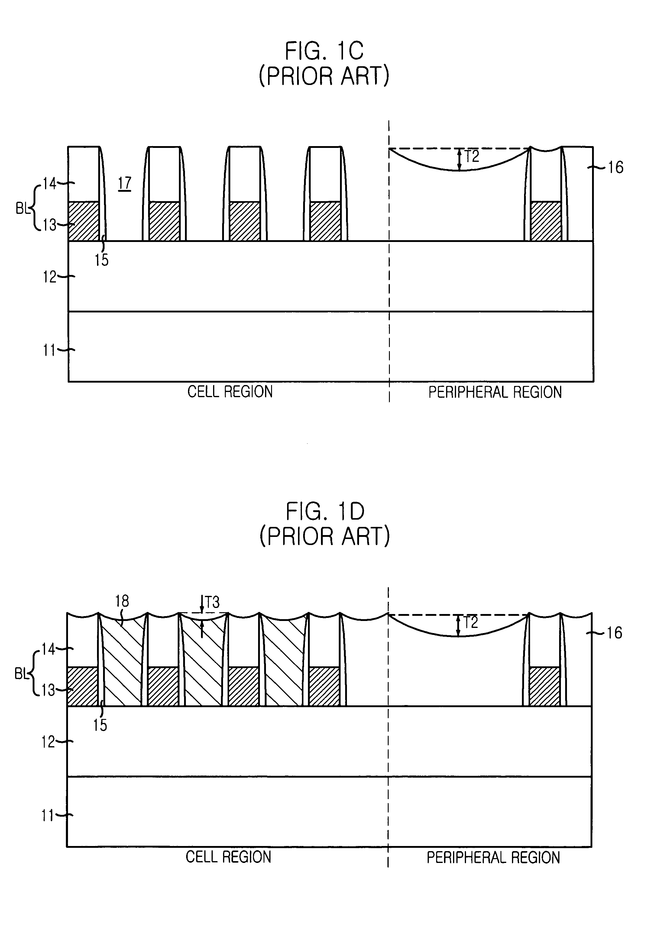
a technology of storage nodes and contacts, which is applied in the direction of semiconductor devices, basic electric elements, electrical appliances, etc., can solve the problems of deteriorating the dishing problem of the plurality of storage nodes, contact failure, and the dishing of the peripheral region with the low pattern density much mor

Inactive Publication Date: 2009-03-24
SK HYNIX INC
View PDF6 Cites 1 Cited by
  • Summary
  • Abstract
  • Description
  • Claims
  • Application Information

AI Technical Summary

Benefits of technology

[0018]It is, therefore, an object of the present invention to provide a method for fabricating a plurality of storage node contacts in a semiconductor device capable of minimizing an influence of a slurry residue and planarizing cruspidal patterns caused during a storage node contact isolation process.

Problems solved by technology

However, even though the conventional method performs the CMP process to remove the cruspidal patterns, the cruspidal patterns still remain and even induce a problem of deteriorating the dishing problem of the plurality of storage node contacts.
Also, slurry impurities remain in the dishing T5 and thus, these slurry impurities cannot be easily removed through a subsequent cleaning process, thereby generating a contact fail.
Furthermore, there is another problem that the dishing of the peripheral region with the low pattern density is much more deteriorated as much as dishing T4, i.e., T4>T2.

Method used


Image

  • Method for fabricating storage node contact in semiconductor device
  • Method for fabricating storage node contact in semiconductor device
  • Method for fabricating storage node contact in semiconductor device

Examples


Embodiment Construction

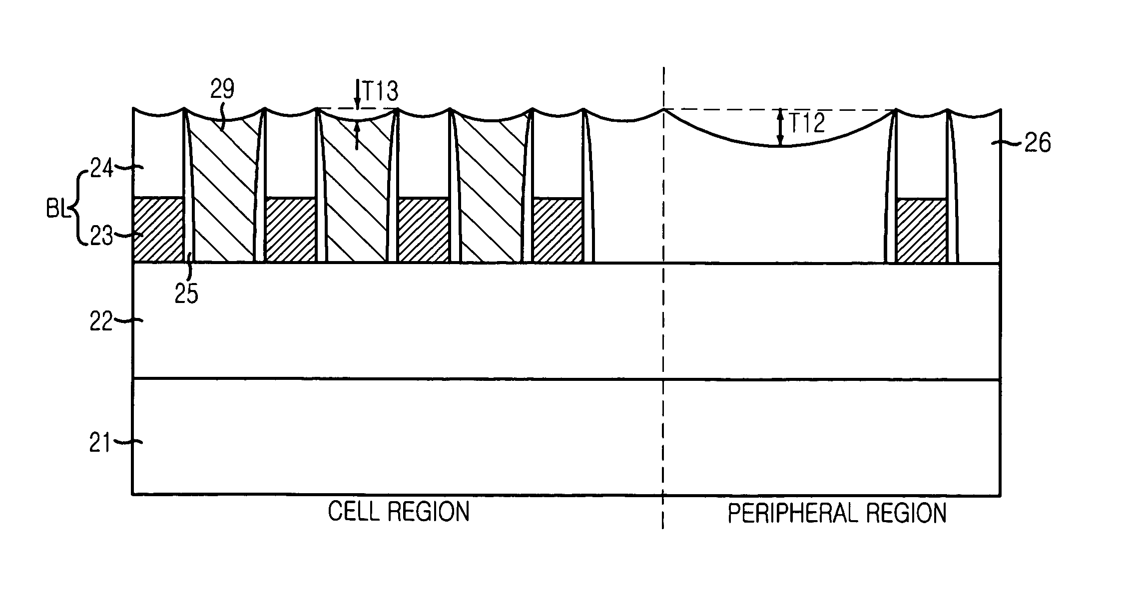
[0025]Hereinafter, detailed descriptions on a preferred embodiment of the present invention will be provided with reference to the accompanying drawings.

[0026]FIG. 2 is a flowchart illustrating a method for fabricating a storage node contact in a semiconductor device in accordance with the present invention.

[0027]Referring to FIG. 2, the method for fabricating the storage node contact in the semiconductor device in accordance with the present invention is performed in the steps of preparing a substrate provided with a first inter-layer insulation layer at step S1, forming a bit line pattern at step S2, forming a bit line spacer at step S3, forming a second inter-layer insulation layer at step S4, performing a first and a second chemical mechanical polishing (CMP) processes to the second inter-layer insulation layer at step S5, forming a storage node contact hole at step S6, depositing a polysilicon layer at step S7, forming a storage node contact through an etch back process at step...


PUM


Abstract

Disclosed is a method for fabricating a plurality of storage node contacts in a semiconductor device capable of minimizing an influence of a slurry residue and planarizing cruspidal patterns caused during a storage node contact isolation process. In accordance with the present invention, a chemical mechanical polishing (CMP) process that is the last process of the storage node contact isolation process is performed by using the slurry without the selectivity or the reverse selectivity, thereby removing the plurality of cruspidal patterns at every interface of the plurality of bit line patterns BL and the plurality of storage node contacts.

Description

FIELD OF THE INVENTION[0001]The present invention relates to a method for fabricating a semiconductor device; and more particularly, to a method for fabricating a storage node contact.DESCRIPTION OF RELATED ARTS[0002]In general, an electrical operation between a capacitor and a bit line is possible through a contact connected to a source / drain region of a transistor during fabricating a semiconductor device.[0003]Recently, as a scale of integration of a semiconductor device has increased, a space between conductive lines such as gate lines has been narrow. Accordingly, a contact process margin has decreased as well. In order to secure the contact process margin, a self aligned contact (SAC) process has been performed.[0004]FIGS. 1A to 1E are cross-sectional views illustrating a conventional method for fabricating a plurality of storage node contacts in a semiconductor device.[0005]Referring to FIG. 1A, a first inter-layer insulation layer 12 is deposited on a substrate completed wit...

Claims


Application Information

Patent Timeline
Patent Type & Authority Patents(United States)
IPC IPC(8): H01L21/4763
CPCH01L21/76819H01L21/7684H01L27/10855H01L27/10894H01L27/10885H10B12/0335H10B12/482H10B12/09H01L21/28
Inventor RYU, CHEOL-HWISHIN, JONG-HAN
Owner SK HYNIX INC
Why Eureka
Try Eureka