Liquid crystal display

a technology of liquid crystal display and liquid crystal, applied in the direction of identification means, digital storage, instruments, etc., can solve the problems of reducing the yield affecting the display effect of liquid crystal display, and increasing the proportion of defects, so as to achieve the effect of increasing the effective display region of the liquid crystal display panel

Inactive Publication Date: 2009-03-24
SAMSUNG DISPLAY CO LTD
View PDF32 Cites 28 Cited by
  • Summary
  • Abstract
  • Description
  • Claims
  • Application Information

AI Technical Summary

Benefits of technology

[0041]Moreover, the integrated driving chip, which has the gate driver for driving the plurality of gate lines and the source driver for driving the plurality of data lines, is disposed on the LCD panel, thereby increasing an effective display region of the LCD panel.

Problems solved by technology

However, a drawback of the Poly-Si TFT-LCD is that it has a relatively complicated manufacturing process.
However, when a plurality of driving chips is formed on a glass substrate as shown in FIG. 2, there are several problems that arise.
First, when a plurality of driving chips is formed on a glass substrate, the defect proportion increases in proportion to the number of the chips formed on the substrate.
As a result, the yield of the LCD decreases because the LCD module is not able to be used, even if a single chip among the plurality of driving chips is defective.
Further, when the defect proportion increases, the process time of the LCD becomes longer, and the productivity thereof becomes lower.
Second, from the standpoint of instrumental structure, the resulting size of the LCD increases by mounting a plurality of chips on the glass substrate.
As a result, the desired high resolution may not be achieved in an LCD having a restricted size requirement.
Third, since the plurality of chips is formed in one side portion adjacent to the LCD panel, the structure of the LCD panel becomes lopsided, and the whole size of the LCD becomes larger.
Fourth, from the standpoint of image displaying characteristics through the LCD panel, a uniformity of image cannot be maintained due to contact resistance between the plurality of chips and the glass substrate.

Method used


Image

  • Liquid crystal display
  • Liquid crystal display
  • Liquid crystal display

Examples


first embodiment

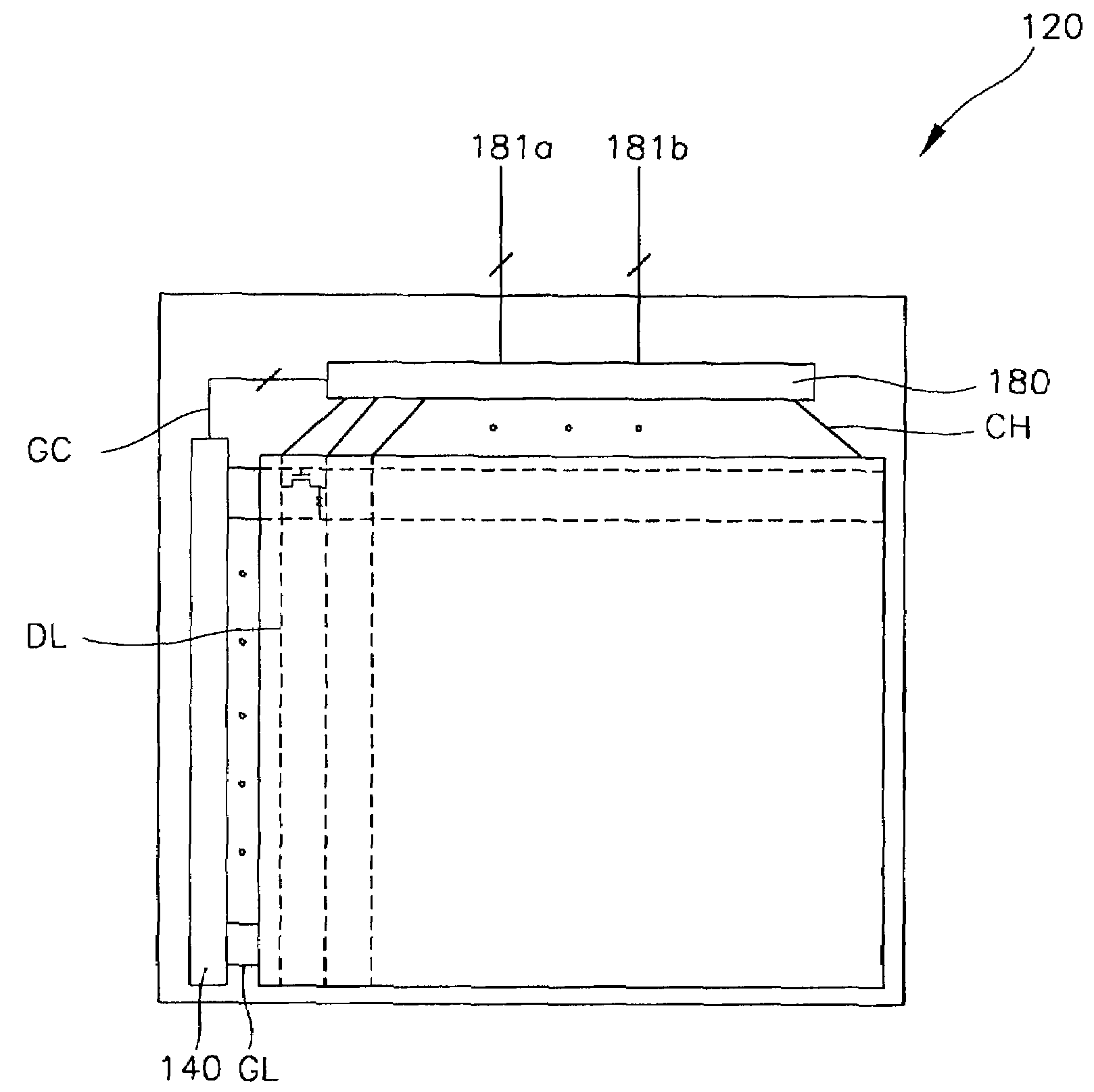
[0074]FIG. 4 is a schematic view showing the TFT substrate shown in FIG. 3 in accordance with the present invention.

[0075]Referring to FIG. 4, the TFT substrate 120 is divided into a first region corresponding to the color filter substrate 130 and a second region not corresponding to the color filter substrate 130. The first region includes a display region and a peripheral region adjacent to the display region. On the display region, there are arranged a plurality of data lines DL extended along the row direction and a plurality of gate lines GL extended along the column direction. A gate driving circuit 140, which is connected to the plurality of gate lines GL, is integrated in the left side of the peripheral region.

[0076]In the second region of the TFT substrate 120, there is arranged the integrated driving chip 180 for controlling the operation of the LCD panel 110. The integrated driving chip 180 receives an external image data signal 181a and an external control signal 181b fr...

second embodiment

[0078]FIG. 5 is a schematic view showing the TFT substrate shown in FIG. 3 in accordance with the present invention.

[0079]Referring to FIG. 5, the TFT substrate 120 is divided into the first region corresponding to the color filter substrate 130 and the second region not corresponding to the color filter substrate 130. The first region includes the display region and the peripheral region adjacent to the display region. On the display region, there are arranged the plurality of data lines DL extended along the row direction and the plurality of gate lines GL extended along the column direction. A gate driving circuit 140 is integrated in the left side of the peripheral region adjacent to the display region, and the gate driving circuit 140 is connected to the plurality of gate lines GL. A line block selecting circuit 150 is integrated in the upper side of the peripheral region, and is connected to the plurality of data lines DL.

[0080]In the second region of the TFT substrate 120, th...

third embodiment

[0139]More specifically, FIG. 18 is a block diagram of a third shift register in the gate driving circuit shown in FIG. 5, according to the present invention. FIG. 19 is a circuit diagram of the third shift register shown in FIG. 18.

[0140]Referring to FIG. 18, the gate driving circuit 140 includes a third shift register 143 that includes a plurality of cascade-connected stages SRC1 through SRCn. Again, the output terminal OUT of each stage is connected to both the input terminal IN of the next stage and the control terminal CT of the previous stage. The third shift register 143 includes n stages corresponding to gate lines GL1 through GLn, with the addition of dummy stage SRCn+1. The dummy stage SRCn+1 provides the control signal to the control terminal CT of the Nth stage SRCn, and operates as a last stage. However, since there is no next stage after the dummy stage, the control terminal CT of the dummy stage SRCn+1 is connected to the fourth node N4 of the Nth stage SRCn.

[0141]Her...


PUM

PropertyMeasurementUnit
DC power voltagesaaaaaaaaaa
power voltageaaaaaaaaaa

Abstract

An LCD capable of being reduced by a whole size and a defective proportion thereof being minimized. An LCD panel of the LCD includes a gate driving circuit that drives gate lines formed extended along a row direction and a line block selecting circuit that drives data lines extended along a column direction. On the LCD panel, an integrated driving chip having a controller, a memory, a level shifter, a source driver, a common voltage generator and a DC/DC converter is mounted. The integrated driving chip not only drives the gate driving circuit and line block selecting circuit, but also controls the operation of the LCD panel to display an image. Thus configured, a defective proportion of the LCD is decreased, with the whole size thereof being reduced.

Description

BACKGROUND OF THE INVENTION[0001]1. Field of the Invention[0002]The present invention relates generally to a liquid crystal display (LCD), and more particularly, to an LCD capable of being reduced by a whole size with a defective proportion thereof being minimized.[0003]2. Description of the Related Art[0004]Information processing devices presently in existence have been rapidly developed to have various architectures, various functions and faster information processing speeds. Information processed in these information processing devices has an electrical signal format. In order to visually confirm the information processed in the information processing device, a display device is typically provided as an interface.[0005]Compared with the traditional cathode ray tube (CRT), liquid crystal displays (LCDs) have certain advantages such as lighter weight, small size, high resolution, and lower power consumption. In addition, LCDs are easily adapted to their intended environment, and ar...

Claims


Application Information

Patent Timeline
Patent Type & Authority Patents(United States)
IPC IPC(8): G02F1/1345G02F1/133G09F9/30G09F9/35G09G3/20G09G3/36
CPCG09G3/3688G11C19/28G09G3/2011G09G2300/0408G09G2300/08G09G2310/0275G09G2310/0297
Inventor KIM, HYUNG-GUELLEE, DONG-HOMA, WON-SEOK
Owner SAMSUNG DISPLAY CO LTD
Why Eureka
Try Eureka