Switch circuit and integrated circuit

a technology of switch circuit and integrated circuit, which is applied in the direction of waveguide type devices, relays, pulse techniques, etc., can solve the problems of deteriorating the distortion characteristics of difficult to achieve sufficiently low distortion characteristics, and inability to obtain excellent distortion characteristics in conventional high frequency switch circuits. achieve excellent distortion characteristics and high voltage resistance characteristics

Active Publication Date: 2009-03-31
FUJITSU LTD
View PDF14 Cites 11 Cited by
  • Summary
  • Abstract
  • Description
  • Claims
  • Application Information

AI Technical Summary

Benefits of technology

[0020]An object of the present invention is to provide a switch circuit with high-voltage resistance characteristics and excellent distortion characteristics.

Problems solved by technology

However, because the mechanical switch wears, it is conceivable that the switch is shifted from the mechanical switch to a switch circuit using a semiconductor element having a high withstand voltage in consideration of reliability, cost, and so on.
In a conventional high frequency switch circuit, however, it is difficult to achieve sufficiently low distortion characteristics.
This greatly deteriorates distortion characteristics of a high frequency switch circuit.
Accordingly, it is impossible to obtain excellent distortion characteristics in the conventional high frequency switch circuit.

Method used


Image

  • Switch circuit and integrated circuit
  • Switch circuit and integrated circuit
  • Switch circuit and integrated circuit

Examples


Embodiment Construction

[0036]Hereinafter, embodiments of the present invention will be described with reference to the drawings.

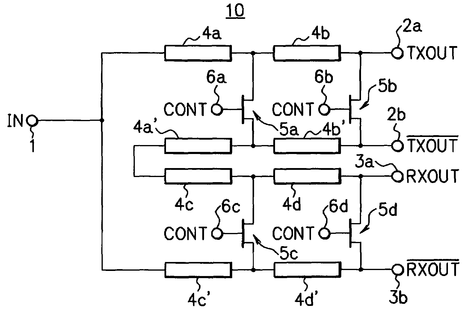
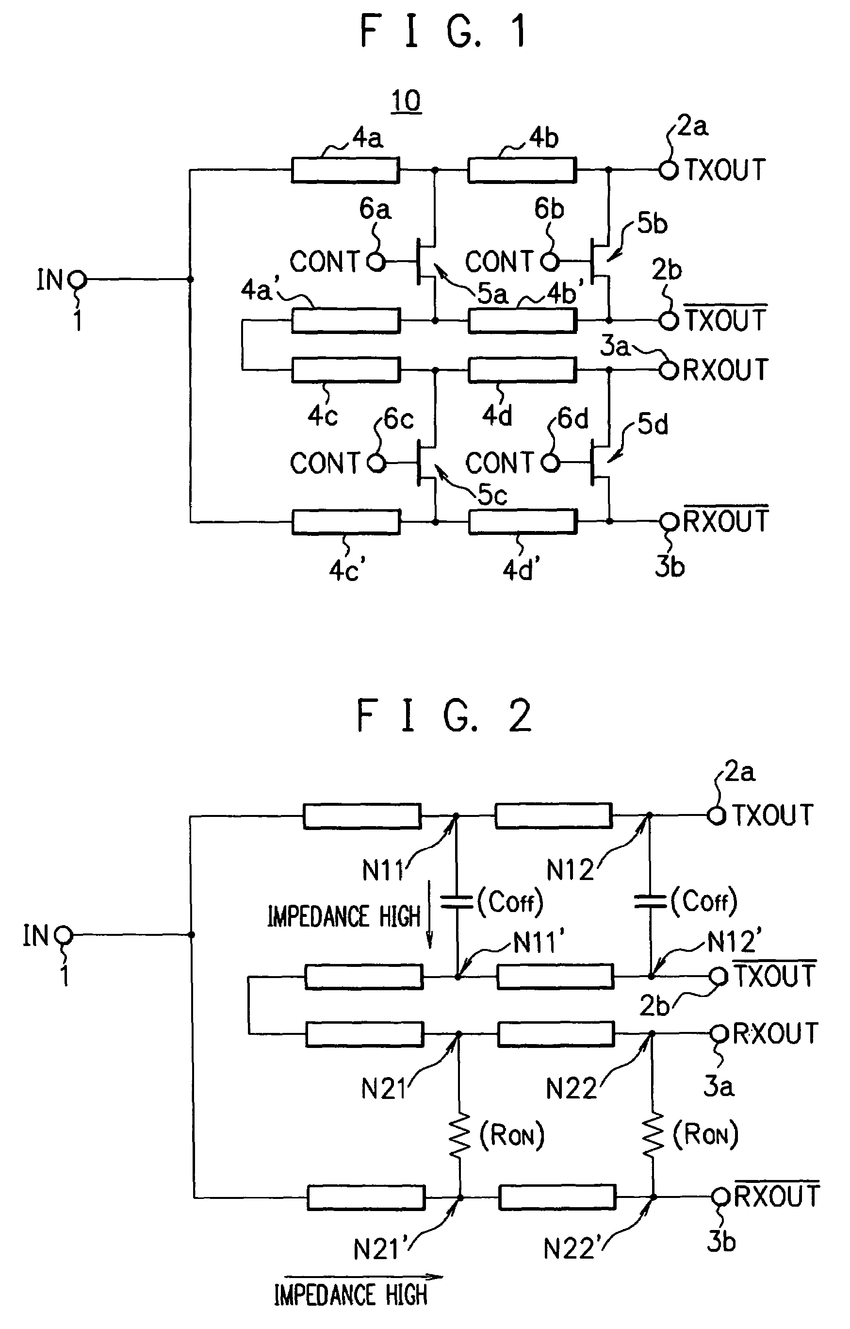
[0037]FIG. 1 is a diagram showing a circuit configuration example of a high frequency switch circuit 10 being one example of a switch circuit according to an embodiment of the present invention. The high frequency switch circuit 10 is a switch circuit operable within a high frequency region and has, as shown in FIG. 1, balanced transmission lines 4a, 4a′, 4b, 4b′, 4c, 4c′, 4d and 4d′ and field effect transistors (FETs) 5a, 5b, 5c, and 5d.

[0038]The high frequency switch circuit 10 further includes an input terminal (IN) 1, transmitting side output terminals (TXOUT, / TXOUT) 2a and 2b, and receiving side output terminals (RXOUT, / RXOUT) 3a and 3b. The input terminal 1 is connected through an unbalanced line and via two branched paths (two balanced transmission lines) to the transmitting side output terminals 2a and 2b and the receiving side output terminals 3a and 3b. On one of the...


PUM


Abstract

A switch circuit includes a balanced line connected between one end of an unbalanced line having another end connected to an input terminal and an output terminal and a balanced line connected between the one end of the unbalanced line and an output terminal. On each of the balanced lines, a plurality of quarter-wave transmission lines are connected in cascade, and each of a plurality of FETs, whose impedance is controllable, is connected between one pair of transmission lines constituting a balanced line for each interconnection point between the transmission lines, so that the power of a signal is distributed to both of the pair of transmission lines, and therefore the inputted power becomes half on each balanced line, thereby making it possible to prevent a DC-like current from flowing when the FET is in an off state even if a high frequency signal with high power is inputted.

Description

CROSS-REFERENCE TO RELATED APPLICATIONS[0001]This application is based upon and claims the benefit of priority from the prior Japanese Patent Application No. 2005-287721, filed on Sep. 30, 2005, the entire contents of which are incorporated herein by reference.BACKGROUND OF THE INVENTION[0002]1. Field of the Invention[0003]The present invention relates to a switch circuit and an integrated circuit and particularly to a circuit preferably used for a high frequency switch circuit used in a high frequency band.[0004]2. Description of the Related Art[0005]In recent years, with the coming of an advanced information society, communication systems such as a wireless LAN and a cellular phone using the high frequency wireless communication technology has come into practical use. To constitute such a communication system, there is a growing demand for high-performance microwave components. For example, in order to realize the communication system with the wireless LAN at a low cost, a module ...

Claims


Application Information

Patent Timeline
Patent Type & Authority Patents(United States)
IPC IPC(8): H01P1/15
CPCH01P1/15H03K17/602H03K17/6271H03K17/693H03K17/76H04B1/48
Inventor INOUE, YUSUKE
Owner FUJITSU LTD
Why Eureka
Try Eureka