
Buffer circuit

a buffer circuit and buffer technology, applied in the field of buffer circuits, can solve the problems of reducing affecting the output voltage response of the output terminal, and affecting the response of the output voltage from the output terminal, so as to reduce the consumption of electricity, reduce power consumption, and increase the driving power

Inactive Publication Date: 2009-04-21
CANON KK
View PDF8 Cites 20 Cited by
  • Summary
  • Abstract
  • Description
  • Claims
  • Application Information

AI Technical Summary

Benefits of technology

The present invention provides a buffer circuit that can balance high capacity driving power, low power consumption, and high-speed output response. The buffer circuit includes an output circuit with two output transistors, two voltage difference detection circuits, and two driving circuits. The driving circuits increase bias current for the output transistors based on the voltage difference detection circuits. The buffer circuit satisfies the trade-off relationship between lowering power consumption and a slew rate characteristic.

Problems solved by technology

That delays response, and accordingly, the response of the output voltage from the output terminal is delayed.
As the current steadily flows, however, it impedes lowering the consumption of the electricity.
As the lower power consumption and the high-speed output response are in trade-off relationship as mentioned above, it has been difficult to realize the buffer circuit that satisfies both of the characteristics.

Method used


Image

  • Buffer circuit
  • Buffer circuit
  • Buffer circuit

Examples


first embodiment

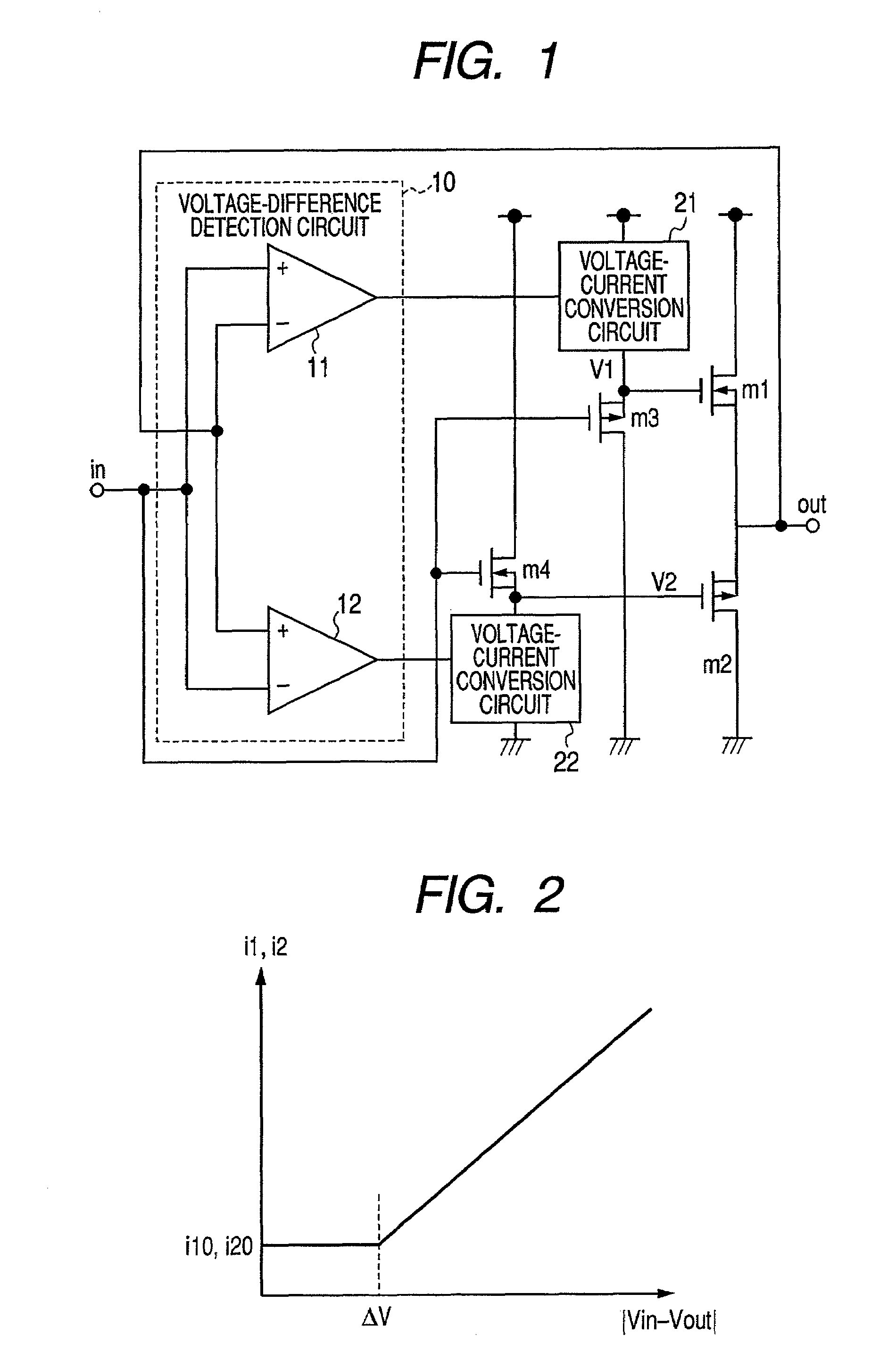
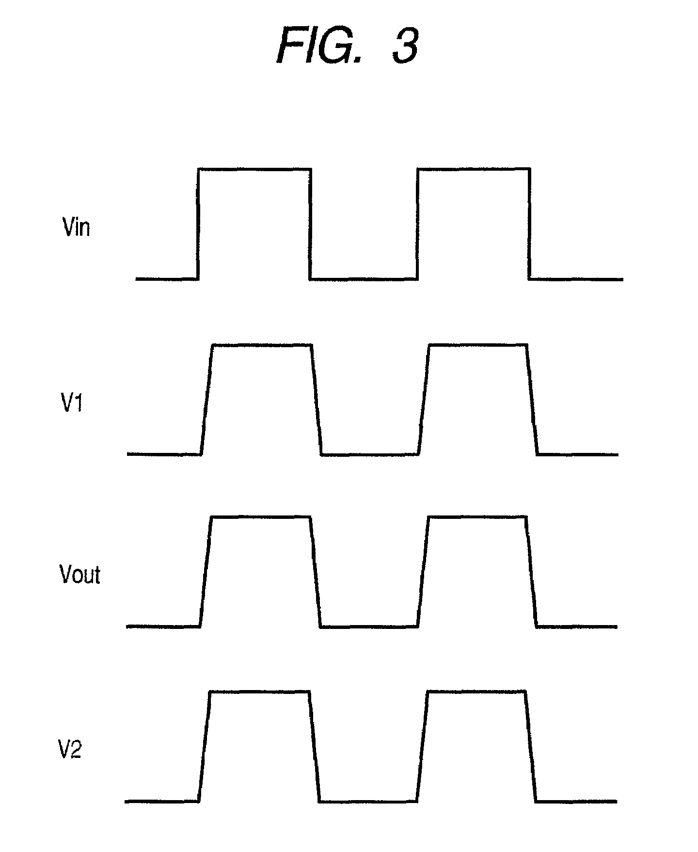
[0023]FIG. 1 is a circuit diagram showing configuration of a first embodiment of a buffer circuit according to the present invention. The circuit shown in FIG. 1 is a buffer circuit for outputting an input voltage input into an input terminal ‘in’ from an output terminal ‘out’ as an output voltage.

[0024]To the output terminal ‘out’ of the buffer circuit, a source terminal of an output NMOS transistor m1 and a source terminal of an output PMOS transistor m2 are connected, forming a push-pull type output circuit. In the description below, each of the MOS transistors is simply referred to as the NMOS or the PMOS for simplicity.

[0025]A drain terminal of an output NMOS m1 forming the output circuit is connected with a power source. Gate terminals are connected with a voltage-current conversion circuit 21 which supplies current from the power source and a source terminal of a PMOS m3. A drain terminal of PMOS m3 is connected with a reference potential and a gate terminal is connected with...

second embodiment

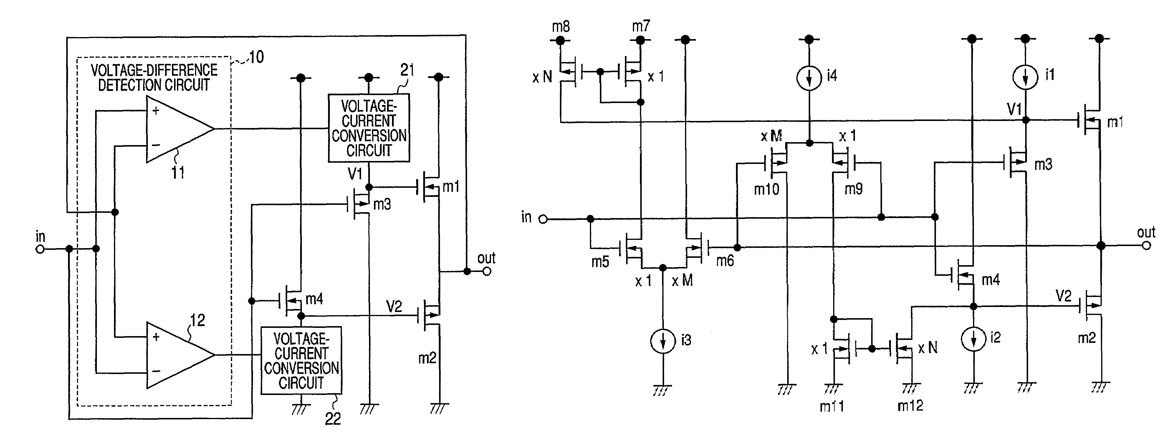
[0051]FIG. 4 is a circuit diagram showing the second embodiment of the buffer circuit of the present invention. In FIG. 4, the same parts as those in FIG. 1 are numbered the same. A circuit including an NMOS m5, NMOS m6 and a current source i3 shown in FIG. 4 corresponds to the differential amplifier circuit 11 shown in FIG. 1. A circuit including a PMOS m9, a PMOS m10 and a current source i4 corresponds to the differential amplifier circuit 12. The differential amplifier circuits are assumed to have the predetermined input offset voltage as shown in FIG. 1.

[0052]A circuit including a PMOS m7, a PMOS m8 and a constant current source i1 shown in FIG. 4 corresponds to the voltage-current conversion circuit 21 shown in FIG. 1. A circuit including an NMOS m11, an NMOS m12 and a constant current source i2 corresponds to the voltage-current conversion circuit 22. The embodiment, however, shows an example of supplying a predetermined bias current instead of characteristic that the bias cur...


PUM


Abstract

The present invention provides a buffer circuit meeting both of low power consumption requirement and an improvement in slew rate characteristics which are in a relation of trade off. Voltage difference detection circuits are provided for detecting a voltage difference between the input signal at rising and at trailing and an output signal. Based on the voltage difference, voltage-current conversion circuits increase a bias current to be supplied to an output NMOS transistor m1 and a source terminal of an output PMOS transistor constituting an output circuit. And, the voltage difference detection circuits have offset voltages. Only when the voltage difference changes into a level higher than the offset voltage, that is, when the input signal changes abruptly (rise or down), bias current increases.

Description

BACKGROUND OF THE INVENTION[0001]1. Field of the Invention[0002]The present invention relates to a buffer circuit and more specifically to a buffer circuit that can improve a slew rate characteristic under a low current consumption.[0003]2. Description of the Related Art[0004]In recent years, in an output buffer circuit used in various driver ICs and the like, a buffer circuit for satisfying characteristics in a trade-off relationship to each other, such as a large capacity driving power, a lower power consumption, and a high-speed output response has been needed.[0005]As a conventional buffer circuit for outputting an input voltage, which is input into an input terminal, from an output terminal as an output voltage, a diamond-shaped buffer circuit, which is disclosed in Japanese Patent Application Laid-Open No. 2002-185269, has been known.[0006]The above buffer circuit is formed by combination of source follower circuits of an output NMOS (N-channel MOS field-effect transistor) and...

Claims


Application Information

Patent Timeline
Patent Type & Authority Patents(United States)
IPC IPC(8): H03B1/00
CPCH03K17/042H03K17/04206H03K17/6874H03K2217/0036
Inventor YAMAZAKI, YOSHIKAZU
Owner CANON KK
Learn More