Magnetoresistive element, magnetoresistive head, magnetic recording apparatus, and magnetic memory

a technology of magnetoresistive head and magnetic recording apparatus, which is applied in the field of magnetoresistive element, magnetoresistive head, magnetic recording apparatus, and magnetic memory, can solve the problems of high element resistance, insufficient metal ccp element to sense very weak fields, and difficult to put to,

Inactive Publication Date: 2009-04-28
KK TOSHIBA
View PDF53 Cites 37 Cited by
  • Summary
  • Abstract
  • Description
  • Claims
  • Application Information

AI Technical Summary

Problems solved by technology

When such a magnetoresistive element is applied to a magnetic head, a higher element resistance poses problems in regard to shot noise and high frequency response.
Accordingly, the metal CCP element is insufficient to sense very weak fields resulting from an increased density and thus hard to put to, practical use.
However, in spite of their good characteristics shown above, the CCP-CPP element is supposed insufficient to sense very weak field signals from a media with a high recording density of 200 to 500 Gbpsi.
Thus, it is difficult to put these elements to practical use.

Method used


Image

  • Magnetoresistive element, magnetoresistive head, magnetic recording apparatus, and magnetic memory
  • Magnetoresistive element, magnetoresistive head, magnetic recording apparatus, and magnetic memory
  • Magnetoresistive element, magnetoresistive head, magnetic recording apparatus, and magnetic memory

Examples


example 1

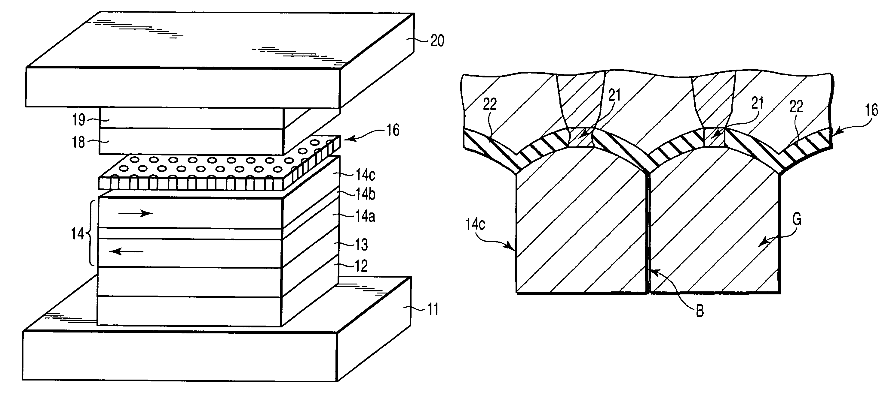
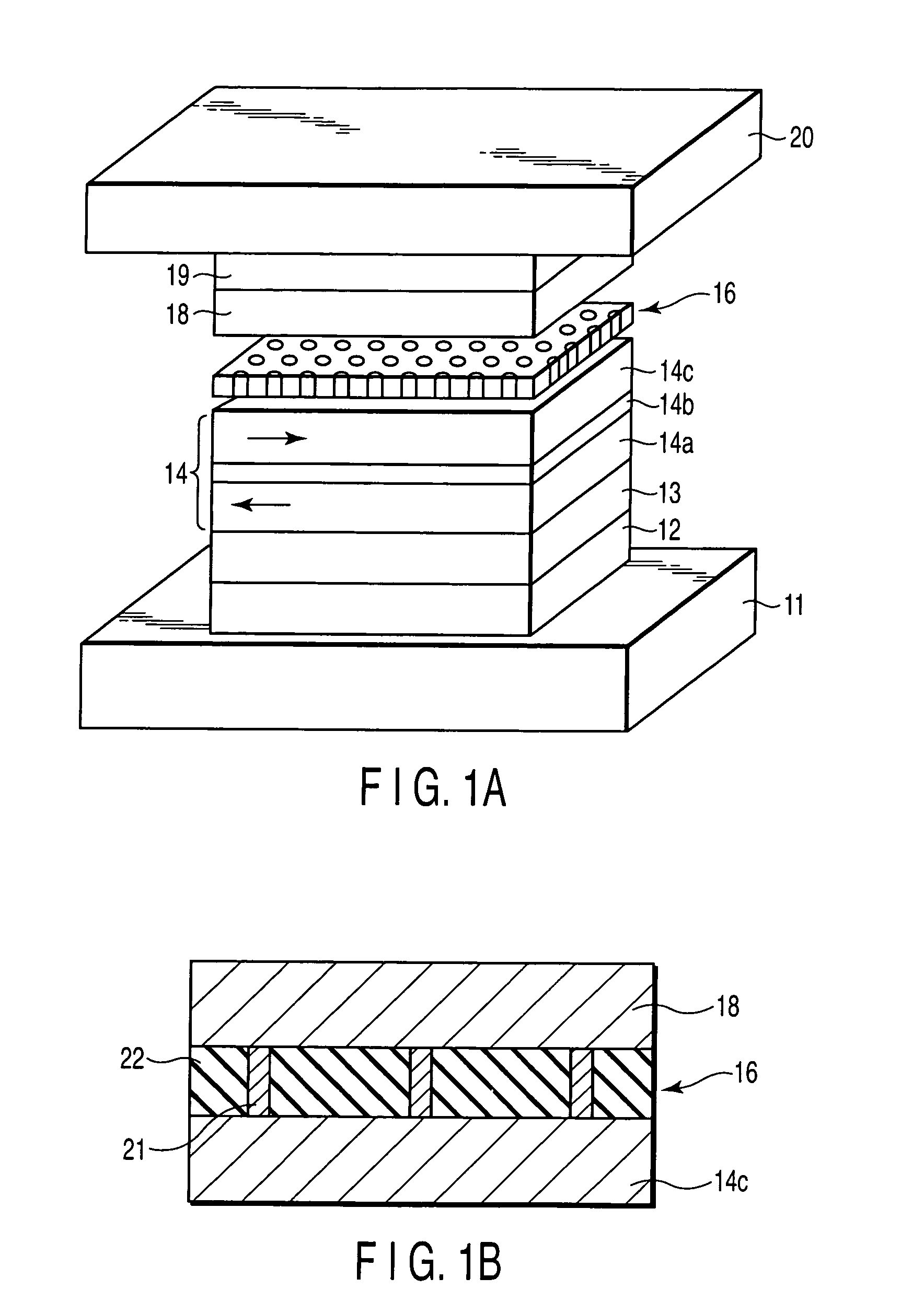
[0053]In the present Example, a magnetoresistive element (CCP-CPP element) having the structure shown in FIG. 1A is manufactured. Specifically, the films mentioned below are sequentially formed on a substrate (not shown):

[0054]lower electrode 11,

[0055]underlayer 12: Ta [5 nm] / Ru [2 nm],

[0056]pinning layer 13: Pt50Mn50 [15 nm],

[0057]pinned layer 14: Co90Fe10 [4 nm] / Ru [0.9 nm] / Co90Fe10 [4 nm],

[0058]lower metal layer 15: Cu [0.5 nm],

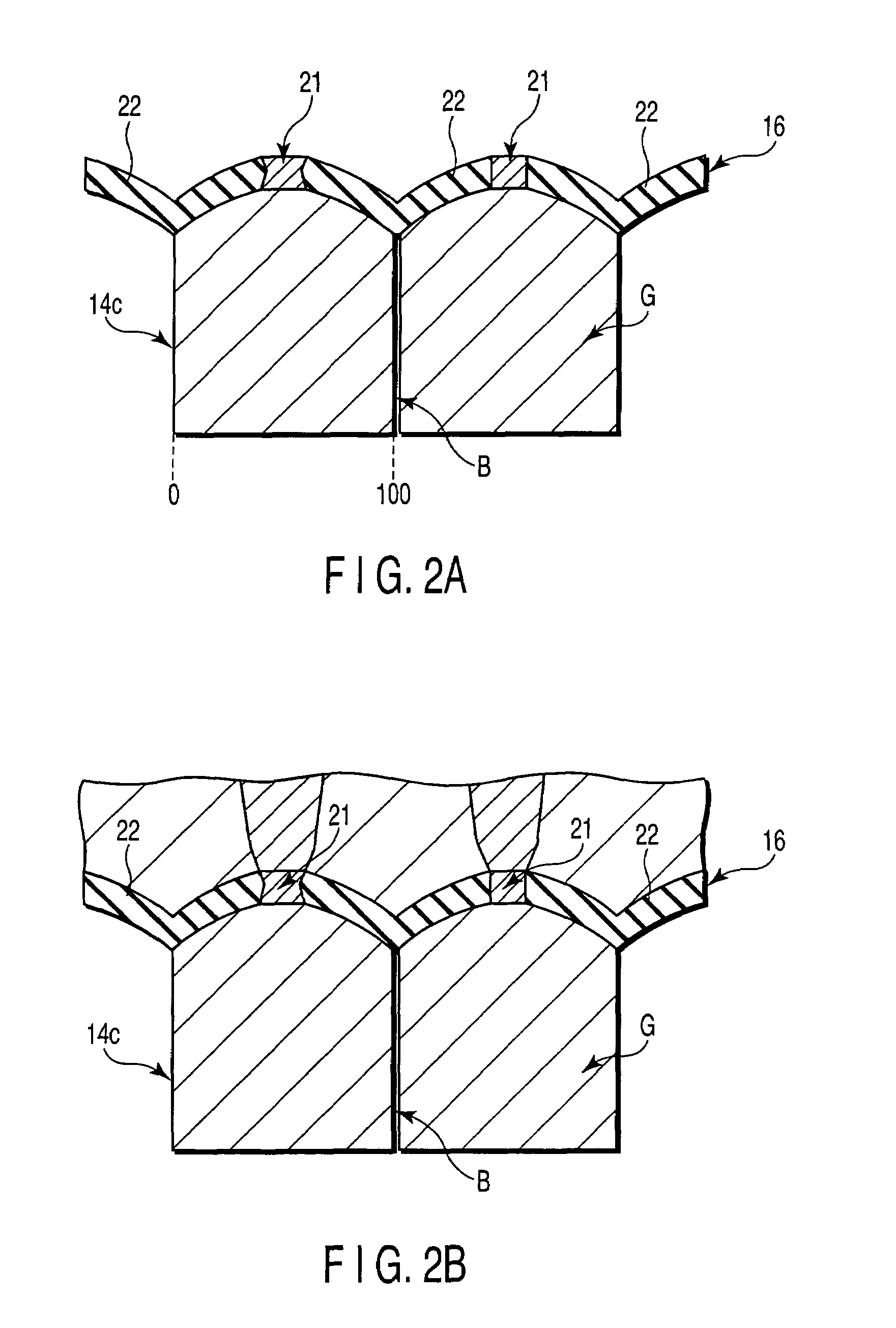
[0059]spacer layer (CCP-NOL) 16: an insulating layer 22 of Al2O3 and current paths 21 of Cu (prepared by depositing Al90Cu10 [0.9 nm], followed by performing PIT and IAO treatments),

[0060]upper metal layer 17: Cu [0.25 nm],

[0061]free layer 18: Co90Fe10 [4 nm],

[0062]cap layer 19: Cu [1 nm] / Ru [10 nm], and

[0063]upper electrode 20.

[0064]In the description below, a set of the spacer layer 16, in a narrow sense, and two metal layers located over and under the spacer layer 16 may be referred to as the spacer layer. The CCP-CPP element in FIG. 1A is of a bottom t...

example 2

[0118]In the present Example, a magnetoresistive element (CCP-CPP element) having the following structure is manufactured:

[0119]lower electrode 11,

[0120]underlayer 12: Ta [5 nm] / Ru [2 nm],

[0121]pinning layer 13: Pt50Mn50 [15 nm],

[0122]pinned layer 14: Co90Fe10 [4 nm] / Ru [0.9 nm] / (Fe50Co50 [1 nm] / Cu [0.25 nm])×2 / Fe50Co50 [1 nm],

[0123]lower metal layer 15: Cu [0.5 nm],

[0124]spacer layer (CCP-NOL) 16: an Al2O3 insulating layer 22 and Cu current paths 21 (prepared by depositing Al90Cu10 [1 nm], followed by performing PIT and IAO treatments, where the PIT / IAO treatments use similar conditions to those of Example 1),

[0125]upper metal layer 17: Cu [0.25 nm],

[0126]free layer 18: Co90Fe10 [1 nm] / Ni83Fe17 [3.5 nm],

[0127]cap layer 19: Cu [1 nm] / Ru [10 nm], and

[0128]upper electrode 20.

[0129]FIGS. 13A and 13B show cross-sectional TEM photographs of the magnetoresistive element (CCP-CPP element) manufactured in the present Example. In FIGS. 13A and 13B, a current path is formed on an almost centr...


PUM

PropertyMeasurementUnit
thicknessaaaaaaaaaa
thicknessaaaaaaaaaa
crystal orientation angleaaaaaaaaaa

Abstract

A magnetoresistive element has a magnetization pinned layer a magnetization direction of which is substantially pinned in one direction, a magnetization free layer a magnetization direction of which varies depending on an external field, and a spacer layer including an insulating layer provided between the magnetization pinned layer and the magnetization free layer and current paths penetrating the insulating layer, the magnetization pinned layer or magnetization free layer located under the spacer layer comprising crystal grains separated by grain boundaries extending across a thickness thereof, in which, supposing that an in-plane position of one end of each of the crystal grains is set to 0 and an in-plane position of a grain boundary adjacent to the other end of the crystal grain is set to 100, the current path corresponding the crystal grain is formed on a region in a range between 20 and 80 of the in-plane position.

Description

CROSS-REFERENCE TO RELATED APPLICATIONS[0001]This application is based upon and claims the benefit of priority from prior Japanese Patent Application No. 2004-325315, filed Nov. 9, 2004, the entire contents of which are incorporated herein by reference.BACKGROUND OF THE INVENTION[0002]1. Field of the Invention[0003]The present invention relates to a magnetoresistive element having a structure in which a sense current is allowed to flow perpendicularly to a plane of a magnetoresistive film, and a magnetoresistive head, a magnetic recording apparatus, and a magnetic memory which use the magnetoresistive element.[0004]2. Description of the Related Art[0005]In recent years, the discovery of a giant magnetoresistive effect (GMR) has rapidly improved the performance of magnetic devices, particularly magnetic heads. In particular, the application of the spin-valve films (SV films) to magnetic heads in or magnetic random access memories (MRAMs) has brought about significant technical improv...

Claims


Application Information

Patent Timeline
Patent Type & Authority Patents(United States)
IPC IPC(8): G11B5/39
CPCB82Y25/00G01R33/093G11B5/3903H01F10/3259H01L43/08G11B5/3929H01L27/224H01L27/228H10B61/10H10B61/22H10N50/10
Inventor FUKUZAWA, HIDEAKIYUASA, HIROMIKOUI, KATSUHIKOIWASAKI, HITOSHI
Owner KK TOSHIBA
Why Eureka
Try Eureka