MEMS structure with anodically bonded silicon-on-insulator substrate

a technology of anodized bonding and silicon on the substrate, which is applied in the direction of microelectromechanical systems, microstructural device assemblies, microstructural systems, etc., can solve the problems of inconvenient use of boron-doped silicon layers, inconvenient fabrication methods, and inconvenient use of thin film deposition and etching

Active Publication Date: 2009-05-05
THE RES FOUND OF STATE UNIV OF NEW YORK
View PDF22 Cites 10 Cited by
  • Summary
  • Abstract
  • Description
  • Claims
  • Application Information

AI Technical Summary

Benefits of technology

[0007]Briefly, the present invention satisfies the need for a well-defined thin silicon membrane for a sensor by incorporating an anodically bonded silicon-on-insulator (SOI) substrate with another substrate, the insulator layer serving as an excellent etch stop.
[0010]It is another object of the present invention to provide a way to create a structure with a SOI substrate anodically bonded on each side to a glass substrate, such that creation of the second anodic bond does not degrade the first anodic bond.
[0016]The present invention provides, in a sixth aspect, a method of making a MEMS structure. The method comprises providing a SOI substrate having a first silicon layer, a second silicon layer and an insulator layer between the first silicon layer and the second silicon layer. The method further comprises anodically bonding a first glass substrate to the SOI substrate at the first silicon layer, thereby creating a first bond, and anodically bonding a second glass substrate to the SOI substrate at the second silicon layer, thereby creating a second bond. The method also comprises preventing debonding of the first bond during creation of the second bond.

Problems solved by technology

But their fabrication is quite a challenge due to the strict requirement of process reproducibility and wafer uniformity.
Conventional fabrication methods have inherent non-uniformity across full wafer size in both thin film deposition and etching.
However, there are three key disadvantages associated with the use of a heavily boron-doped silicon layer.
One is that the boron doping process requires a long drive-in time.
If the silicon membrane thickness is large, it becomes practically impossible to fabricate a freely suspended membrane.
The second disadvantage is that the etch chemical is very toxic to allow an acceptable etch stop on boron-doped silicon.
Heavy silicon doping also introduces stress into the fabricated silicon membrane and performance degradation can result.

Method used


Image

  • MEMS structure with anodically bonded silicon-on-insulator substrate
  • MEMS structure with anodically bonded silicon-on-insulator substrate
  • MEMS structure with anodically bonded silicon-on-insulator substrate

Examples


Embodiment Construction

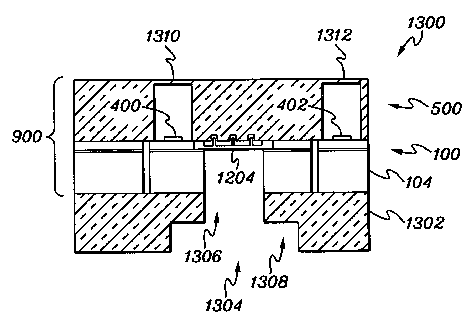
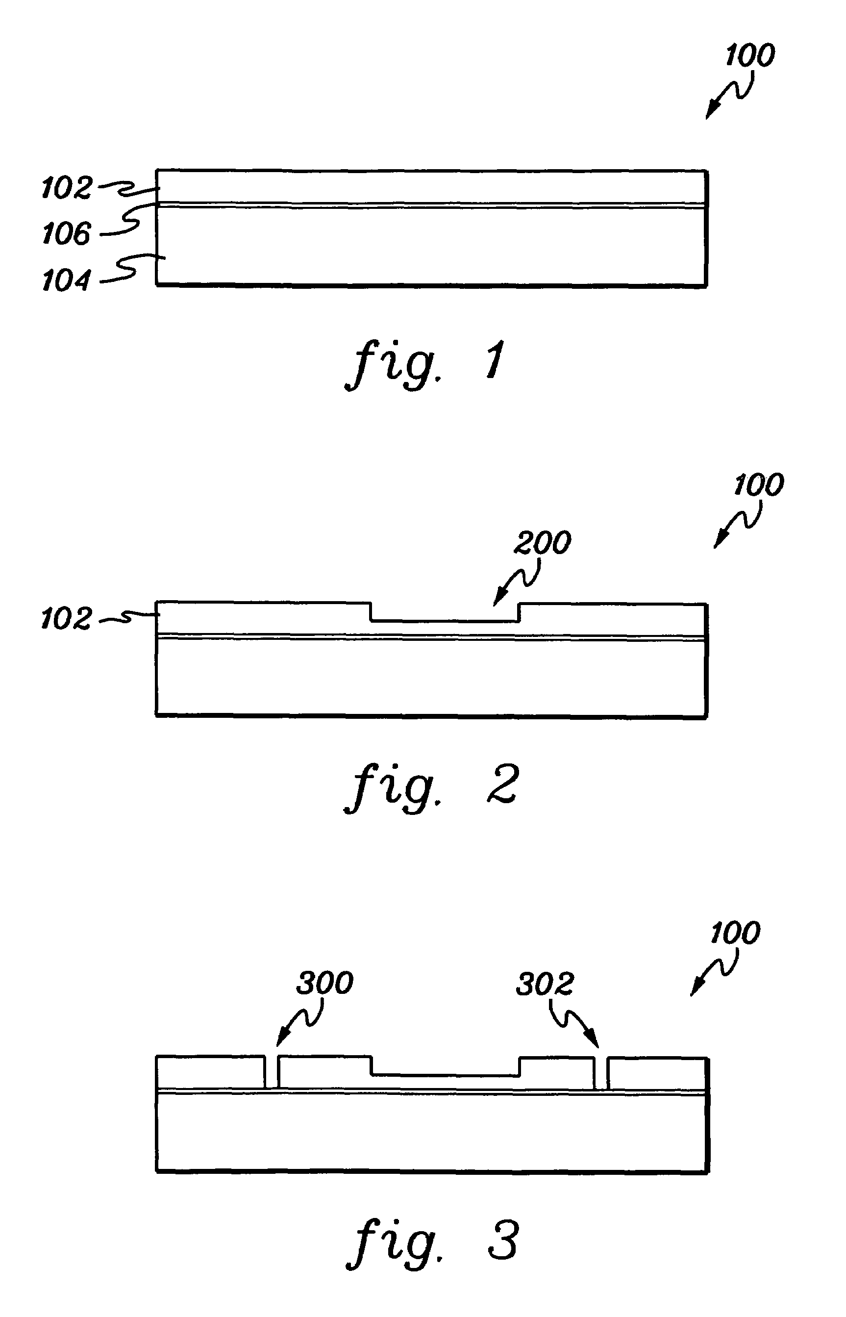
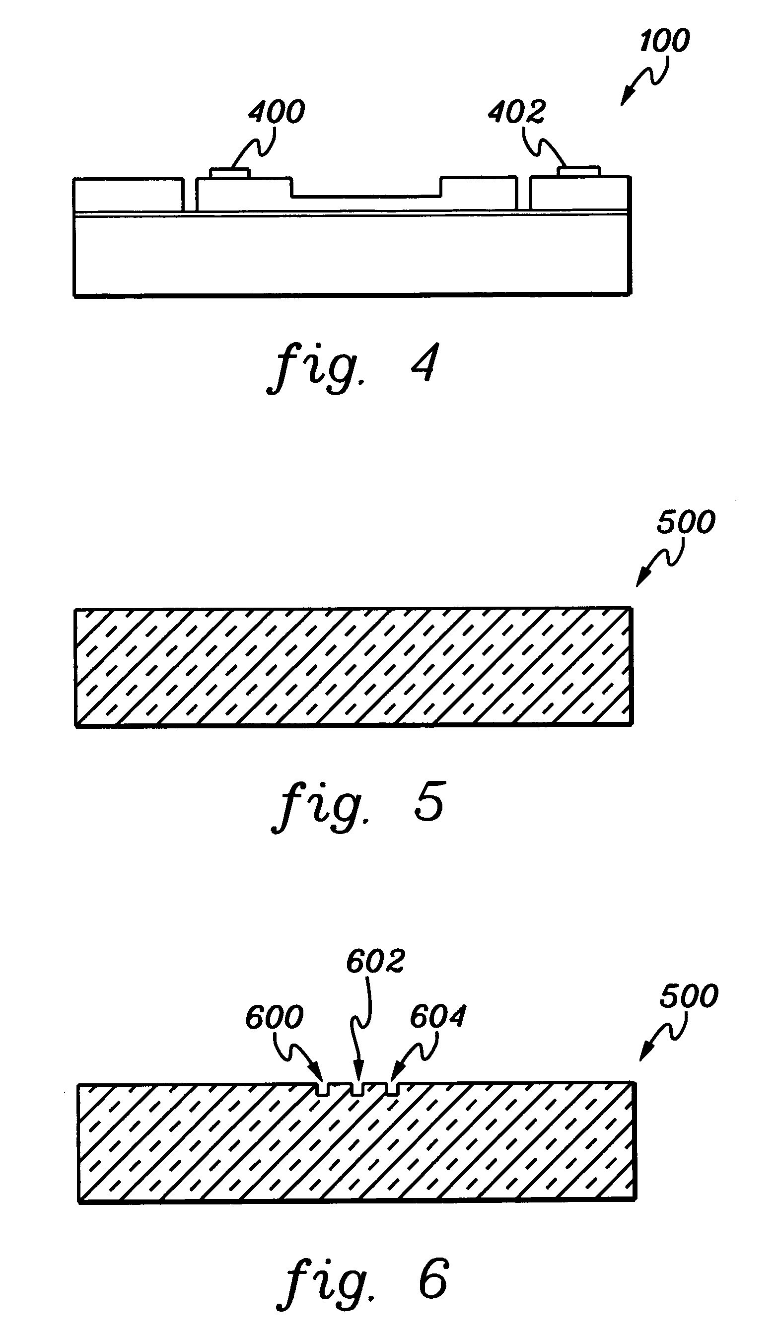
[0034]FIG. 1 is a cross-sectional view of a silicon-on-insulator (SOI) substrate 100 prior to processing thereof in accordance with the present invention. SOI substrate 100 comprises a first silicon layer 102, also referred to as the device layer, a second silicon layer 104, also referred to as the handle layer, and an insulator layer 106 therebetween. The insulator layer comprises silicon dioxide (SiO2).

[0035]FIG. 2 depicts the SOI substrate 100 of FIG. 1 after photoresist patterning and etching to create a recess 200 in the device layer 102.

[0036]FIG. 3 depicts the SOI substrate 100 of FIG. 2 after the creation of trenches 300 and 302. The trenches are created, for example, by photoresist patterning and etching, using, for example, a Bosch process known in the art. As one skilled in the art will know, the Bosch process involves a sequence of alternating etch and deposition to fabricate high aspect ratio silicon structures while the substrate temperature is controlled near room tem...


PUM


Abstract

A silicon-on-insulator (SOI) substrate is anodically bonded to a glass substrate in a MEMS structure with or without electrically bypassing the insulator layer by electrically comprising the silicon layers. The insulator layer serves as an etch stop to create a well-defined, thin silicon membrane for a sensor. A second glass substrate is anodically bonded to the other side of the SOI substrate, and debonding of the existing anodic bond prevented by eliminating any potential drop across the existing bonded surface.

Description

BACKGROUND OF THE INVENTION[0001]1. Technical Field[0002]The present invention generally relates to Micro-Electro-Mechanical Systems (MEMS). More particularly, the present invention relates to a MEMS structure including an anodically bonded silicon-on-insulator substrate.[0003]2. Background Information[0004]There has been a wide range of fabrication methods developed to fabricate microsensors and microactuators. These devices can be used for sensing, measurement and displacement in the range of micrometers or sub-micrometers. The sensitivity of such kind of devices can be high because of their extremely small dimensions. But their fabrication is quite a challenge due to the strict requirement of process reproducibility and wafer uniformity. Conventional fabrication methods have inherent non-uniformity across full wafer size in both thin film deposition and etching.[0005]It is a common practice to form a heavily B-doped silicon layer and use this as an etch stop to construct a thin s...

Claims


Application Information

Patent Timeline
Patent Type & Authority Patents(United States)
IPC IPC(8): H01L21/00
CPCB81C3/001B81B2201/0292B81C2203/031
Inventor XU, BAITOKRANOVA, NATALYACASTRACANE, JAMES
Owner THE RES FOUND OF STATE UNIV OF NEW YORK
Why Eureka
Try Eureka