Semiconductor device including regions of band-engineered semiconductor superlattice to reduce device-on resistance

a semiconductor superlattice and semiconductor technology, applied in the field of semiconductor devices, can solve the problems of significant inefficiency in the resistance to carrier flow in semiconductor devices, and achieve the effect of reducing the resistance of carrier flow

Inactive Publication Date: 2009-05-12
ATOMERA INC
View PDF63 Cites 85 Cited by
  • Summary
  • Abstract
  • Description
  • Claims
  • Application Information

AI Technical Summary

Problems solved by technology

The resistance to carrier flow in semiconductor devices is a significant source of inefficiency, particularly in majority carrier devices such as metal-oxide semiconductor field-effect transistors (MOSFETs).

Method used


Image

  • Semiconductor device including regions of band-engineered semiconductor superlattice to reduce device-on resistance
  • Semiconductor device including regions of band-engineered semiconductor superlattice to reduce device-on resistance
  • Semiconductor device including regions of band-engineered semiconductor superlattice to reduce device-on resistance

Examples


Embodiment Construction

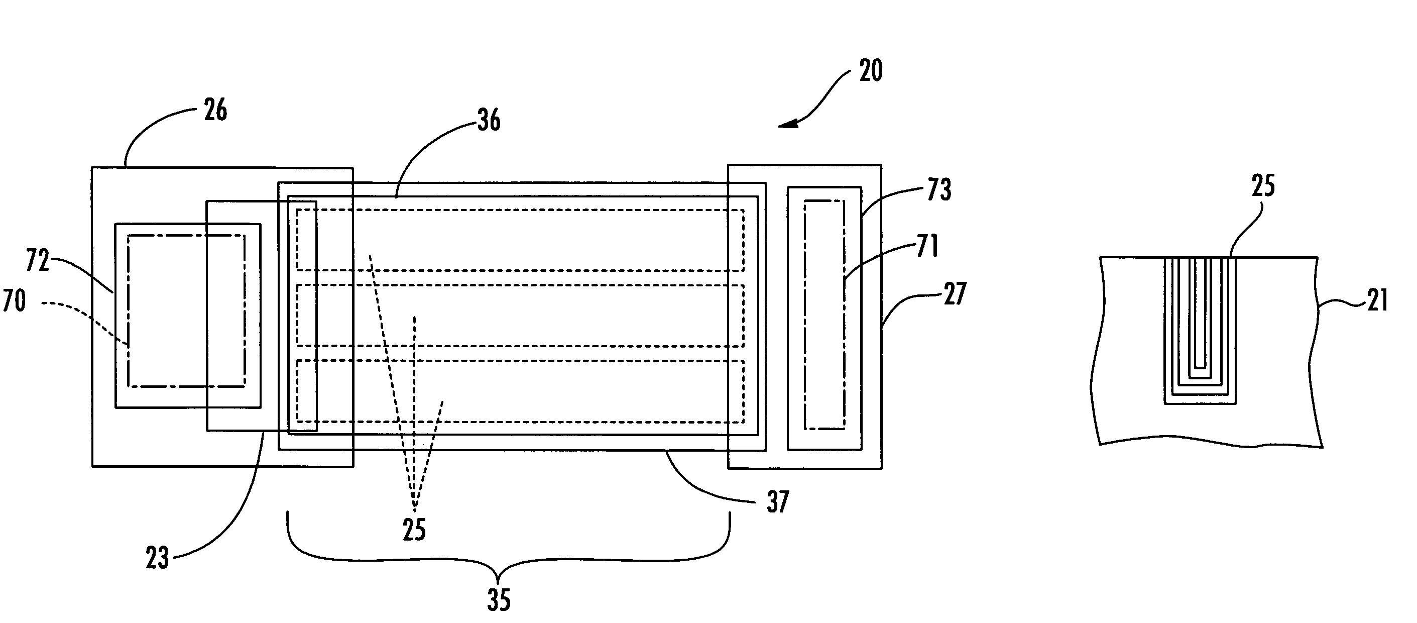
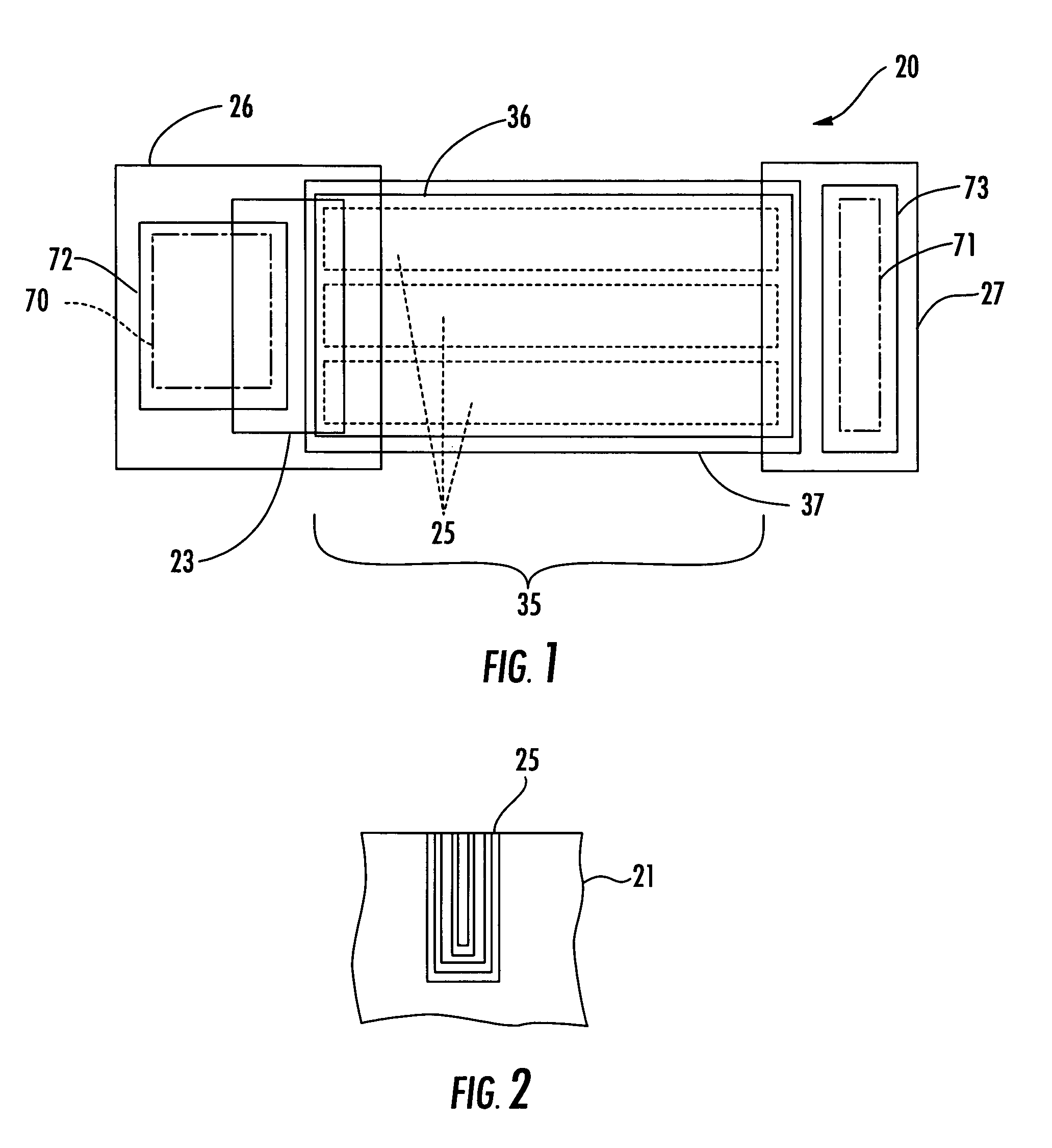
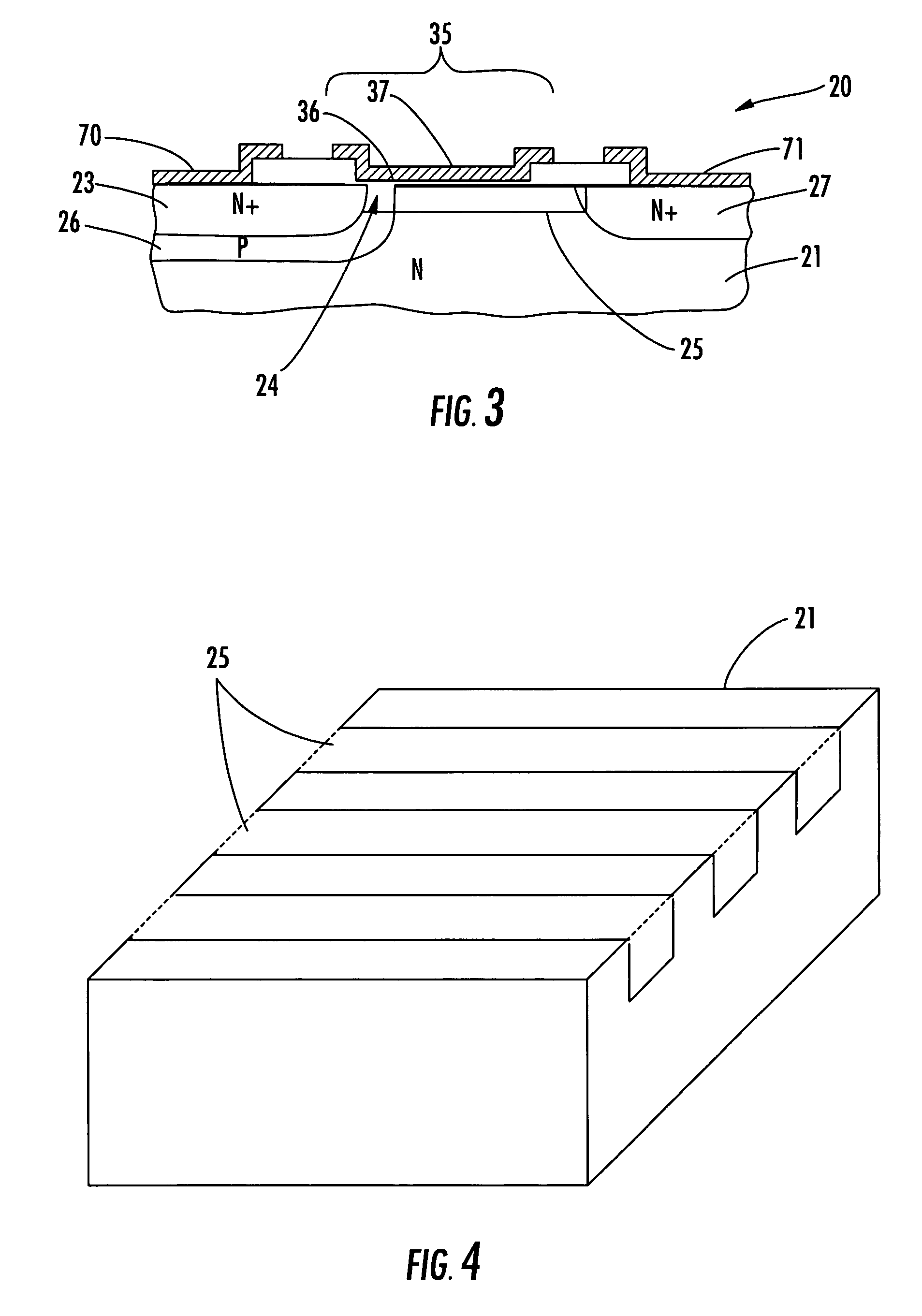
[0034]The present invention will now be described more fully hereinafter with reference to the accompanying drawings, in which preferred embodiments of the invention are shown. This invention may, however, be embodied in many different forms and should not be construed as limited to the embodiments set forth herein. Rather, these embodiments are provided so that this disclosure will be thorough and complete, and will fully convey the scope of the invention to those skilled in the art. Like numbers refer to like elements throughout, and prime notation is used to indicate similar elements in alternative embodiments.

[0035]The present invention relates to controlling the properties of semiconductor materials at the atomic or molecular level to achieve improved performance within semiconductor devices. Further, the invention relates to the identification, creation, and use of improved materials for use in semiconductor devices. In particular, the following description discusses the incor...


PUM


Abstract

A semiconductor device may include a substrate and spaced apart source and drain regions defining a channel region therebetween in the substrate. The substrate may have a plurality of spaced apart superlattices in the channel and / or drain regions. Each superlattice may include a plurality of stacked groups of layers, with each group including a plurality of stacked base semiconductor monolayers defining a base semiconductor portion and at least one non-semiconductor monolayer thereon. The at least one non-semiconductor monolayer may be constrained within a crystal lattice of adjacent base semiconductor portions.

Description

CROSS-REFERENCE TO RELATED APPLICATIONS[0001]This application claims the benefit of U.S. Provisional Application No. 60 / 720,302, filed Sep. 23, 2005, and is a continuation-in-part of U.S. patent application Ser. No. 10 / 940,426 filed Sep. 14, 2004, now U.S. Pat. No. 7,436,026 which is a continuation of U.S. patent application Ser. No. 10 / 647,069 filed Aug. 22, 2003, now U.S. Pat. No. 6,897,472, which is a continuation-in-part of U.S. patent application Ser. Nos. 10 / 603,696 and 10 / 603,621 filed on Jun. 26, 2003, now abandoned the entire disclosures of which are incorporated by reference herein.FIELD OF THE INVENTION[0002]The present invention relates to the field of semiconductors, and, more particularly, to semiconductors having enhanced properties based upon energy band engineering and associated methods.BACKGROUND OF THE INVENTION[0003]Structures and techniques have been proposed to enhance the performance of semiconductor devices, such as by enhancing the mobility of the charge ca...

Claims


Application Information

Patent Timeline
Patent Type & Authority Patents(United States)
IPC IPC(8): H01L29/06
CPCB82Y10/00H01L29/1054H01L29/152H01L29/158H01L29/66568H01L29/66681H01L29/66712H01L29/66734H01L29/7802H01L29/7813H01L29/7816H01L29/0873
Inventor BLANCHARD, RICHARD A.
Owner ATOMERA INC
Why Eureka
Try Eureka