Light emitting diode driving circuit and optical transmitter for use in optical fiber link

a driving circuit and light-emitting diode technology, applied in the field of optical transmitters, can solve the problems of low current consumption, distortion of pulse width, and difficulty in accelerating the response speed of led emitting light, and achieve the effect of easy realization of low current consumption

Active Publication Date: 2009-05-12
SHARP KK
View PDF3 Cites 2 Cited by
  • Summary
  • Abstract
  • Description
  • Claims
  • Application Information

AI Technical Summary

Benefits of technology

[0014]In view of the foregoing problems, the present invention was made, and an object of the present invention is to provide a light emitting diode driving circuit that easily realizes low current consumption and high-speed light emission for the LED, and to provide an optical transmitter for use in an optical fiber link adopting such a light emitting diode driving circuit.
[0016]In the foregoing configuration, in the case where the ON / OFF signal is at a voltage level (e.g. ground electrical potential) that causes the light emitting diode to emit light, a drive current supplied to the first MOS or bipolar transistor is mirrored at a predetermined ratio, and flows into the light emitting diode and the second MOS or bipolar transistor. At the same time, a peaking current is supplied from the peaking circuit to the light emitting diode. That is, the current that flows into the LED is produced by overlapping the peaking current with the current that flows into the second MOS or bipolar transistor, and therefore the current so produced is peaked (current with a waveform whose rising and falling edges have a peak point). This allows the LED to be turned ON or OFF at high speed.
[0017]Further, the ON / OFF signal simultaneously causes (i) switching in the current mirror circuit for supplying the driving current to the light emitting diode and (switching whether to supply the driving current to the LED from the second MOS or bipolar transistor), and (ii) switching in the peaking circuit for generating the peaking current (switching whether to supply the peaking current to the LED). Thus, it is possible to match the rising timing and falling timing of the driving current with the rising timing and falling timing of the peaking current, respectively. As a result, a waveform of the current flowing into the light emitting diode is accurately peaked, thereby easily increasing the response speed of the LED emitting light.
[0018]Further, with the foregoing configuration, it is possible to freely adjust the value of the peaking current by suitably setting the characteristics of elements constituting the peaking circuit. For example, in the case where the peaking circuit has a capacitor and a resistor being serially connected with each other, the value of the peaking current can be freely adjusted by suitably setting the capacitance of the capacitor and the resistance of the resistor. This allows an optimum peaking amount to be set for different combinations of the LED and the LED driving circuit. Thus, the response speed of the LED emitting light is easily increased.
[0019]Further, in the foregoing configuration, since switching of the driving current from the drive current source is carried out by the current mirror circuit, the driving current does not flow into the current mirror circuit while the light emitting diode is OFF. This allows for reduction of current consumption.
[0020]Further, since switching of the driving current from the drive current source is carried out by the current mirror circuit, it is possible to accurately regulate a current value of the driving current, and to reduce fluctuations in the current value of the driving current.

Problems solved by technology

This causes a difficulty in reducing current consumption.
Further, due to a delay in an inverter INV3, the peaking current lags behind the driving current.
This may cause distortion in a pulse width, which, in turn, may cause difficulties in accelerating the response speed of the LED emitting light.
This causes difficulties in controlling a peaking amount (height of a rising peak), which, in turn, may cause difficulties in accelerating the response speed of the LED emitting light.
As described, the differential drive type LED driving circuit shown in FIG. 10 is suitable for high speed driving; however, a constant flow of the driving current in the differential circuit causes difficulties in reducing current consumption.
Further, it is difficult to match the ON / OFF timing of the driving current with the ON / OFF timing of the peaking current.
Therefore, it is difficult to accelerate the response speed of the LED emitting light.
Thus, it is difficult to accelerate the response speed of the LED emitting light.

Method used


Image

  • Light emitting diode driving circuit and optical transmitter for use in optical fiber link
  • Light emitting diode driving circuit and optical transmitter for use in optical fiber link
  • Light emitting diode driving circuit and optical transmitter for use in optical fiber link

Examples


embodiment 1

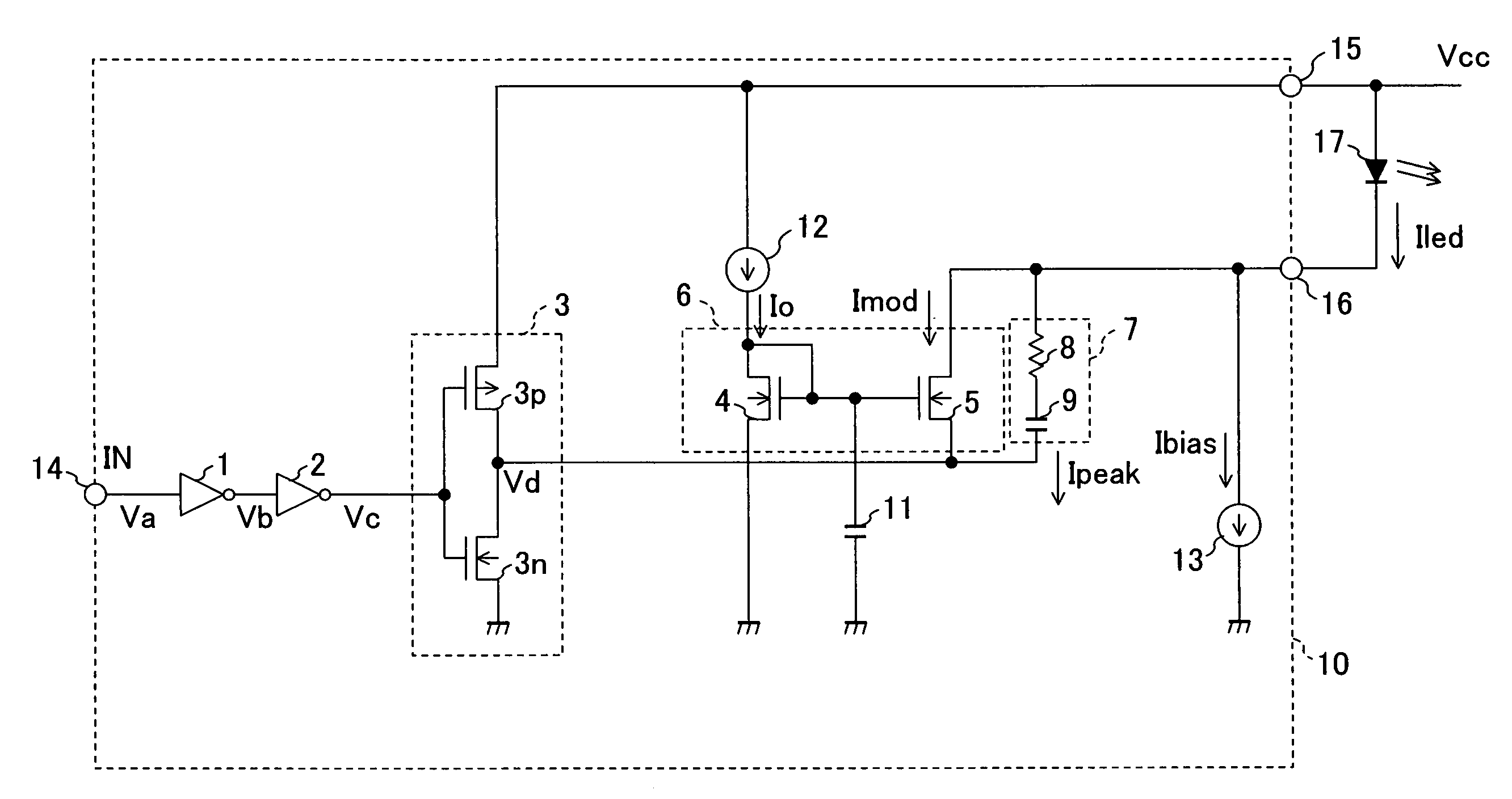
[0035]The following is a detailed description of an embodiment in accordance with the present invention with reference to the drawings. FIG. 1 shows an embodiment of the present invention, and is a block diagram showing a configuration of an optical transmitter for use in the optical fiber link.

[0036]The optical transmitter for use in the optical fiber link of the present invention is provided with an LED (light emitting diode) 17 and an LED driving circuit 10 for driving the LED 17. The LED driving circuit 10 is provided with an input terminal (IN) 14 to which an input electronic signal IN is inputted, a power source terminal (VCC) 15 connected with a constant voltage source (not shown) for outputting a power source voltage Vcc, and an LED connection terminal (LED OUT) 16 to which the LED 17 is connected. One end of the LED 17 is connected with the power source terminal 15, and the other end of the LED 17 is connected with the LED connection terminal 16.

[0037]The input electronic s...

embodiment 2

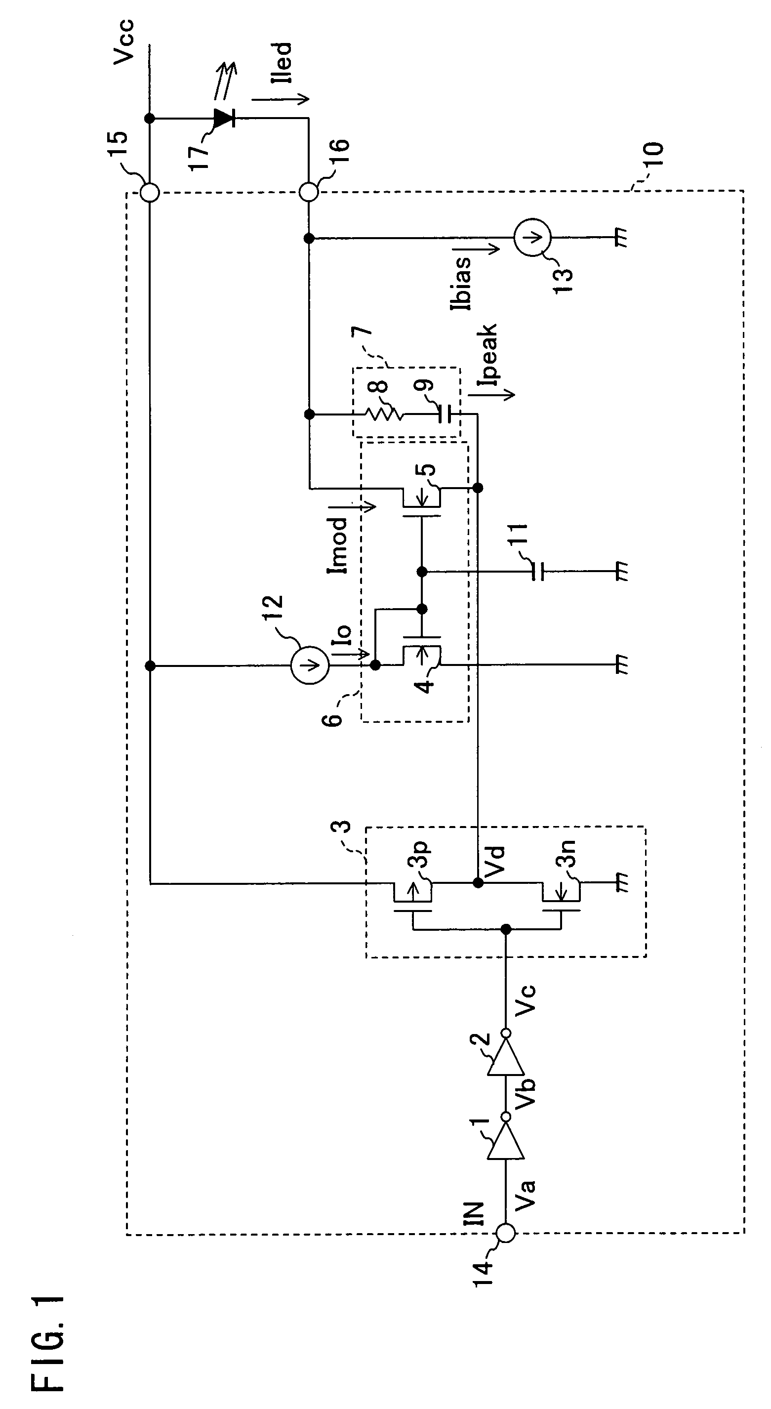
[0049]Another embodiment of the present invention is described below with reference to FIG. 2. Note that the same reference numerals and symbols are given to the members that have the same functions as those described in the foregoing embodiment 1, and descriptions of those members are omitted here as a matter of convenience.

[0050]As shown in FIG. 2, a configuration of an LED driving circuit 20 of the present embodiment is the same as the configuration of the LED driving circuit 10 of the foregoing embodiment 1, except in that the current mirror circuit 6 having the N-channel MOS transistor 4 and the N-channel MOS transistor 5 is replaced with a current mirror circuit 26 having a bipolar NPN transistor (QN) 24 serving as a first bipolar transistor, and a bipolar NPN transistor 25 serving as a second bipolar transistor.

[0051]In this case, a base and a collector of the bipolar NPN transistor 24 are connected with a base of the bipolar NPN transistor 25. Further, an emitter of the bipo...

embodiment 3

[0053]Still another embodiment of the present invention is described below with reference to FIG. 4. Note that the same reference numerals and symbols are given to the members that have the same functions as those described in the foregoing embodiment 1, and descriptions of those members are omitted here as a matter of convenience.

[0054]In the LED driving circuit 10 of the foregoing embodiment 1, a current Imod flows into the output terminal of the inverter 3, when an output voltage Vd from the inverter 3 is low level. More specifically, when the output voltage Vd from the inverter 3 is low level, the N-channel MOS transistor 3n in the inverter 3 is turned on, and therefore the Imod flows between the drain and source of the N-channel MOS transistor 3n. The output voltage does not become GND level (0) completely, due to an on-resistance of the N-channel MOS transistor 3n. When Ron(3n) is the on-resistance of the N-channel MOS transistor 3n, the output voltage from the inverter 3 (a v...


PUM


Abstract

An LED driving circuit includes: (a) a current mirror circuit having N-channel MOS transistors whose respective gates are connected with each other, (b) a constant current source for supplying an LED driving current to an N-channel MOS transistor 4, (c) an LED connection terminal, connected with the N-channel MOS transistors, for connecting the LED, (d) an inverter and an input-terminal respectively for inputting, to a source of the N-channel MOS transistor, an ON / OFF signal for controlling ON / OFF of the LED, and (e) a peaking circuit, connected with a drain and source of the N-channel MOS transistor, for generating a peaking current used in peaking a current flowing into the LED. With this arrangement, it is possible to provide an LED driving circuit that easily realizes low current consumption and high-speed emission for the LED. With such an LED driving circuit, an optical transmitter for use in an optical fiber link can also be realized.

Description

[0001]This Nonprovisional application claims priority under 35 U.S.C. §119(a) on Patent Application No. 2004 / 028693 filed in Japan on Feb. 4, 2004, the entire contents of which are hereby incorporated by reference.FIELD OF THE INVENTION[0002]The present invention relates to an optical transmitter, for use in an optical fiber link, having a light emitting diode (hereinafter referred to as LED) serving as a light emitting element, examples of such optical transmitters including an optical transmitter for use in digital audio equipment, an optical transmitter for use in an in-vehicle optical fiber link, and an optical transmitter for use in a high-speed photo-coupler. The present invention also relates to an LED driving circuit which is suitable for use in such an optical transmitter.BACKGROUND OF THE INVENTION[0003]An optical fiber link (a link utilizing an optical fiber) has been widely used in common house holds, particularly for music-related purposes. The optical fiber link is use...

Claims


Application Information

Patent Timeline
Patent Type & Authority Patents(United States)
IPC IPC(8): H04B10/00G09G3/32H01L33/00H03K17/78H04B10/43H05B37/00H05B44/00
CPCH05B33/0818H05B33/0854Y02B20/347H05B45/18H01L25/167G09G3/32H05B45/32Y02B20/30H05B31/50
Inventor SHIMIZU, TAKAYUKI
Owner SHARP KK
Why Eureka
Try Eureka