Laser addressed monolithic display

a monolithic display and laser technology, applied in lasers, color televisions, solid-state devices, etc., can solve the problems of affecting the dissipation speed of the reverse bias region and the rapid trapping of the electron arriving from the reverse bias region

Active Publication Date: 2009-05-26
OLA DISPLAY
View PDF25 Cites 2 Cited by
  • Summary
  • Abstract
  • Description
  • Claims
  • Application Information

AI Technical Summary

Benefits of technology

[0004]The NPN device operates in the presence of an external electric field across it, which biases its two P-N junctions as reverse biased and forward biased. As the LASER strikes the device on its P-type photosensitive region, charged pairs of electrons and holes are produced and are pulled apart by the cumulative electric field present at the reverse bias region. The holes thus produced reduce the forward bias barrier allowing for a large amount of holes to cross into an emissive N-type region. The emissive region allows this large influx of holes to recombine, with electrons coming due to the external electric field, and emit light. In another embodiment of the invention there is an electron blocker barrier at the forward biased junction that blocks the incoming electrons, due to the external field, to cross over the lowered forward bias barrier and retains them in the emissive region. A similar function is performed by a hole blocker, which retains the in coming holes in the flux by blocking the flow to go out of the emissive region in the external circuit. This retention of electrons and holes allows more time for recombination.
[0006]In another embodiment, the N-type material forming the Schottky contact is a material M1. The properties of the M1 allow for a slower dissipation of charge in the region of the Schottky contact such that it enables a continuous light output by the pixel for a frame period or more even after the scan. In yet another embodiment, the M1 material is replaced by M3 material having an extra trap energy level. Electrons arriving from the reverse bias region get trapped quickly and take longer to dissipate. This action allows continuous light output by the pixel as before.
[0009]In another embodiment, applicable to the NPN and the PNP assemblies, the P-type photosensitive region is only sensitive to infrared light and the scanning LASER is therefore infrared. However, the emissive region being only a visible light emitter inhibits any feedback effects as the emitted light becomes incident on the photosensitive region. In still a further embodiment, the P-type photosensitive region is also photosensitive to visible light. This allows a feedback effect to take place whereby the emitted visible light incident on the photosensitive material produces charged pairs just like the incident LASER. This feedback effect enables the LASER addressed area, functioning like a pixel; to remain lighted for a frame period or more or until the external electric field is switched off. In another embodiment, applicable to NPN assembly, we replace the function of the P-type photosensitive region by a N-type photosensitive material forming the Schottky barrier and with the feedback mechanism, just described, being active. In the PNP case, the N-type photosensitive layer forms the reverse bias junction and is placed alongside the N-type emissive material. In the NPN case, a regular P-type material is used in place of the previous P-type photosensitive region. In another embodiment, with a visible light N-type emitter, the photosensitive region is sensitive to visible light and the photosensitive area of the device is either a P-type or a N-type material as in previous embodiments. In addition, there is a filter placed as such that the emitted visible light coming from the display area and other ambient light is filtered, without affecting the LASER, for a select narrow band of visible light to strike the photosensitive area and provide a feedback effect.

Problems solved by technology

Electrons arriving from the reverse bias region get trapped quickly and take longer to dissipate.

Method used


Image

  • Laser addressed monolithic display
  • Laser addressed monolithic display
  • Laser addressed monolithic display

Examples


Embodiment Construction

[0031]To facilitate description any numeral identifying an element in one figure will represent the same element in any other figure.

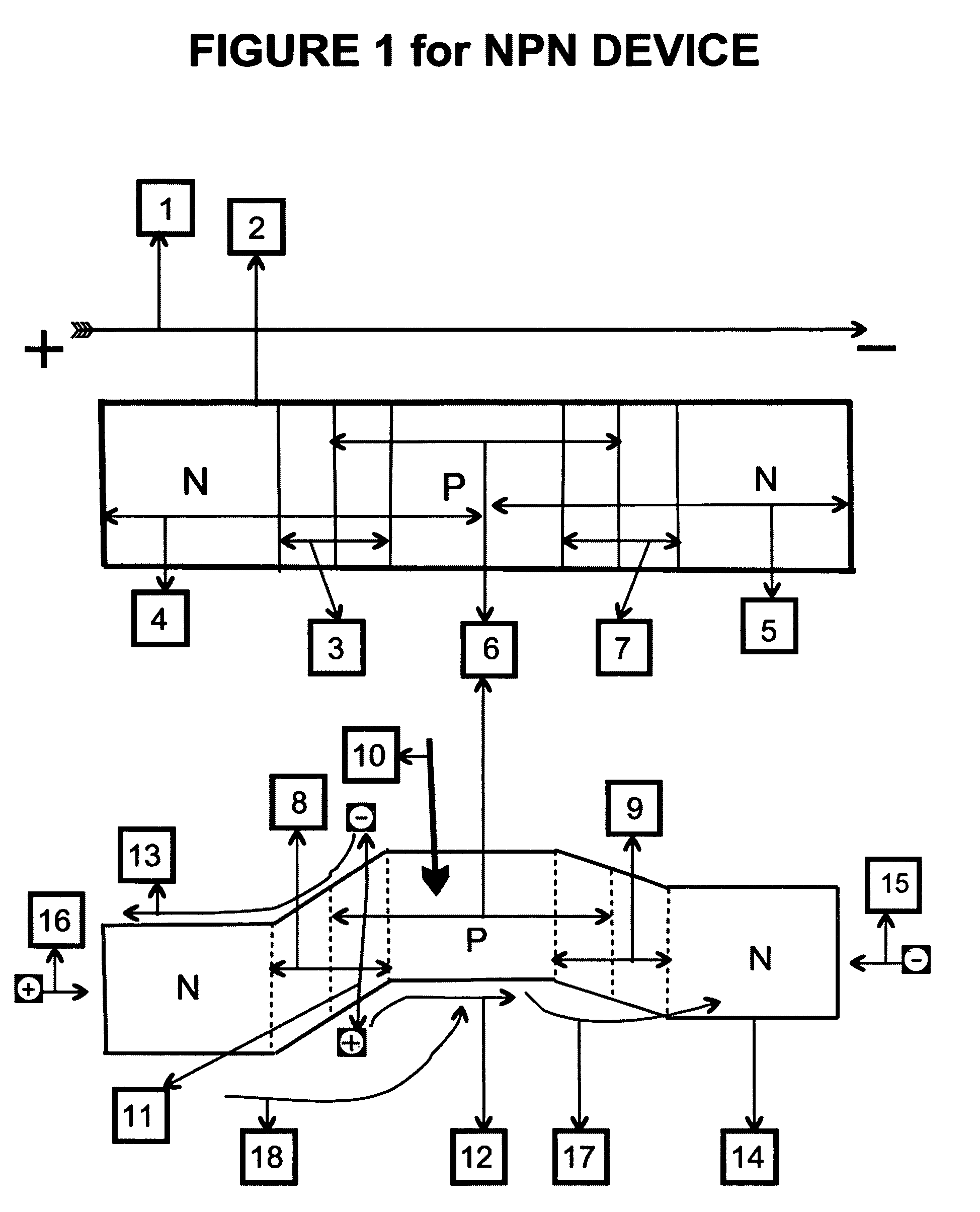
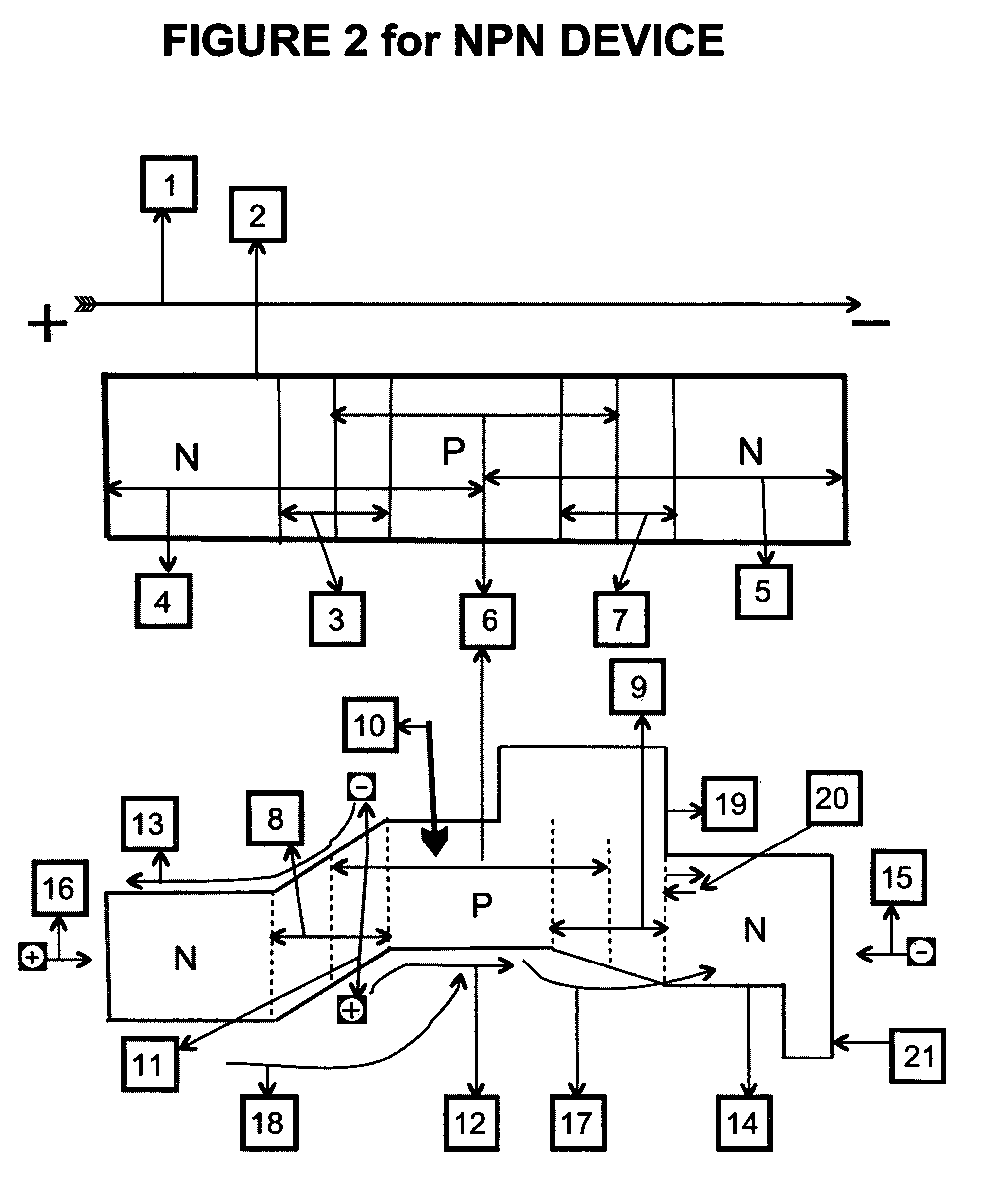
[0032]FIG. 20 and FIG. 21 represent the functioning of the proposed display screen 34. Light is emitted 49 from the screen 34 only from the area illuminated by the laser. This area performs as a photo-amplifying and light-emitting device 48 or 50 as will be described in detail in the following. As the light emission occurs only from a restricted area, at a certain time this creates the equivalent of an addressed pixel. By scanning the LASER 10 across the screen 34, we can generate and address all pixels on the screen.

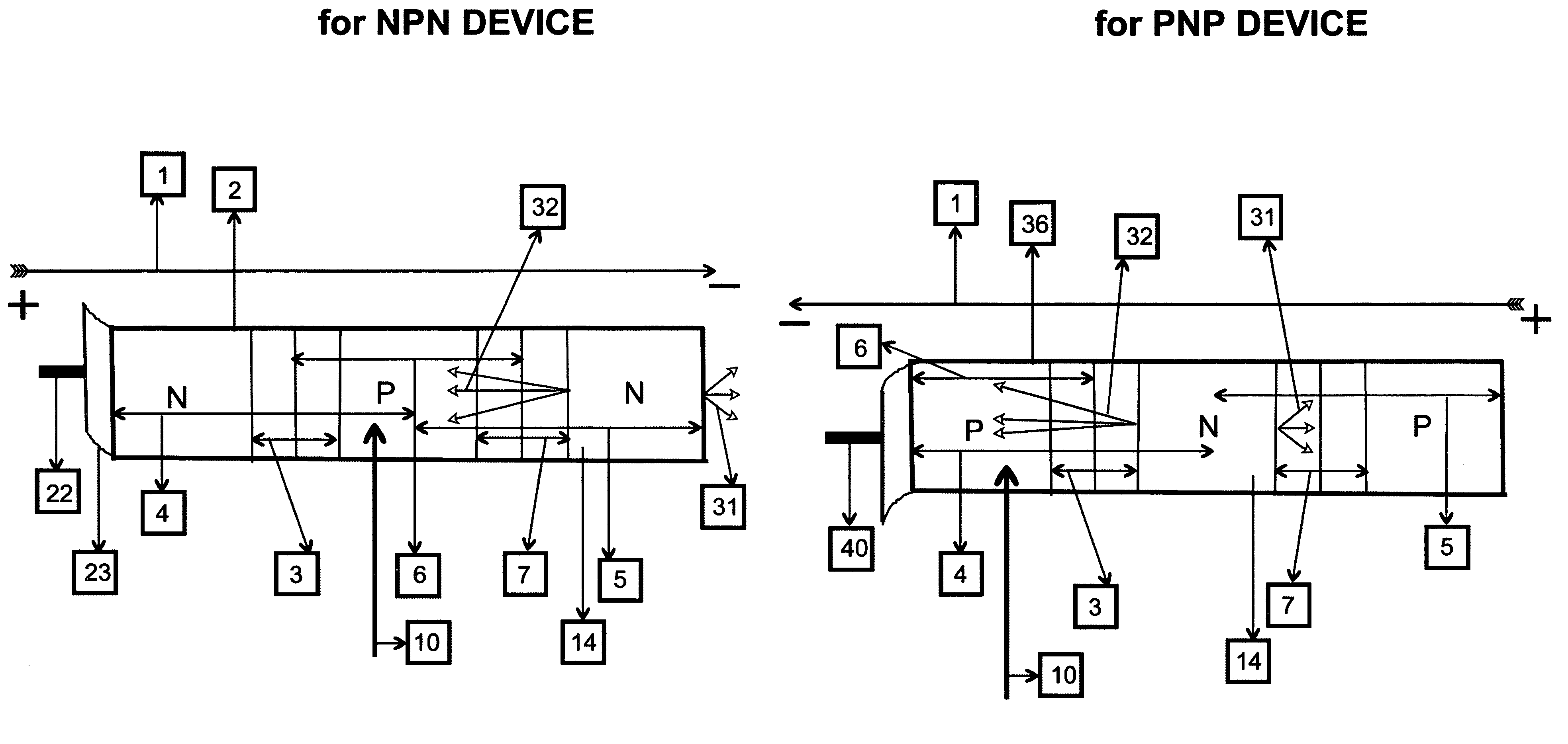
[0033]In case of a first embodiment, with reference to FIG. 1 and FIG. 12, we have NPN and PNP photo-amplifying and light-emitting devices respectively. Both devices use negatively charged electrons and positively charged holes as carriers of current. Both devices in FIG. 1 and FIG. 12 have an external electric field 1 across it and in thi...


PUM


Abstract

The present invention aims to provide a display screen where pixels are addressed by a scanning LASER. The screen performs as a photo-amplifier circuit, producing light output at the region being illuminated by the LASER. This illumination produces electron-hole pairs forming two small currents, one of which subsequently results in a much larger electron or hole current from a specific region of the photo-amplifier. This larger current reaches an emitting region where recombination with other electrons or holes produces light. The duration of the light output is increased up to a frame period or more by increasing the duration of the larger current using various materials having properties that prolong recombination of electrons and holes in a specific device region. In another instance, a feedback effect is utilized by using the incident output light, which may be filtered, replacing the scanning LASER that has left the pixel.

Description

BACKGROUND OF THE INVENTION[0001]The invention relates to a monolithic display device, scanned by a laser in presence of an applied electric field, comprised of a light-sensing area and a light-emitting area such that an amplification of carriers within the device causes an emission of light. This emission of light is made to persist a frame period or more using carrier blocking materials, light-emitted feedback loop and materials with trap energy levels.[0002]Prior art of the invention would involve projection type displays vastly different from the present invention, as these do not utilize a scanning laser to energize pixels on the display screen. Other prior art would involve display which use laser as the light source but not to energize pixels such as U.S. Pat. No. 6,636,274 and U.S. Pat. No. 6,594,090.BRIEF SUMMARY OF THE INVENTION[0003]The present invention relates to a display device utilizing a scanning LASER for addressing the area where it is intended to induce light out...

Claims


Application Information

Patent Timeline
Patent Type & Authority Patents(United States)
IPC IPC(8): H01L27/15H01S3/00
CPCH01L27/288H04N9/3129H01L27/3241H10K65/00H10K59/10
Inventor TULI, RAJA SINGHIZQUIERDO, RICARDO
Owner OLA DISPLAY
Why Eureka
Try Eureka