Floating body semiconductor memory device and method of operating the same

a floating body, semiconductor technology, applied in the direction of information storage, static storage, digital storage, etc., can solve the problems of complex operation and control limited layout size of semiconductor memory devices, and capacitor dissipation of capacitors

Active Publication Date: 2009-05-26
SAMSUNG ELECTRONICS CO LTD
View PDF11 Cites 99 Cited by
  • Summary
  • Abstract
  • Description
  • Claims
  • Application Information

AI Technical Summary

Problems solved by technology

However, the capacitor charge dissipates after a predetermined time lapses, and thus the capacitor needs to be periodically refreshed (re-stored).
A semiconductor memory device, which has a memory cell array including dynamic memory cells having such capacitors, is limited with respect to reducing the semiconductor memory device layout size.
However, conventional semiconductor memory devices having floating body memory cells have complicated circuit configurations, which include, for example, reference memory cells, level limiters, sense amplifiers (current sense amplifiers), comparators, latches, and write back gates, in order to perform a read operation, as shown in FIG. 1.
Also, the operation and control of such semiconductor memory devices are complicated.

Method used


Image

  • Floating body semiconductor memory device and method of operating the same
  • Floating body semiconductor memory device and method of operating the same
  • Floating body semiconductor memory device and method of operating the same

Examples


Embodiment Construction

[0035]The present invention will now be described more fully with reference to the accompanying drawings, in which exemplary embodiments of the invention are shown. The invention, however, may be embodied in various different forms, and should not be construed as being limited only to the illustrated embodiments. Rather, these embodiments are provided as examples, to convey the concept of the invention to one skilled in the art. Accordingly, known processes, elements, and techniques are not described with respect to some of the embodiments of the present invention. Throughout the drawings and written description, like reference numerals will be used to refer to like or similar elements.

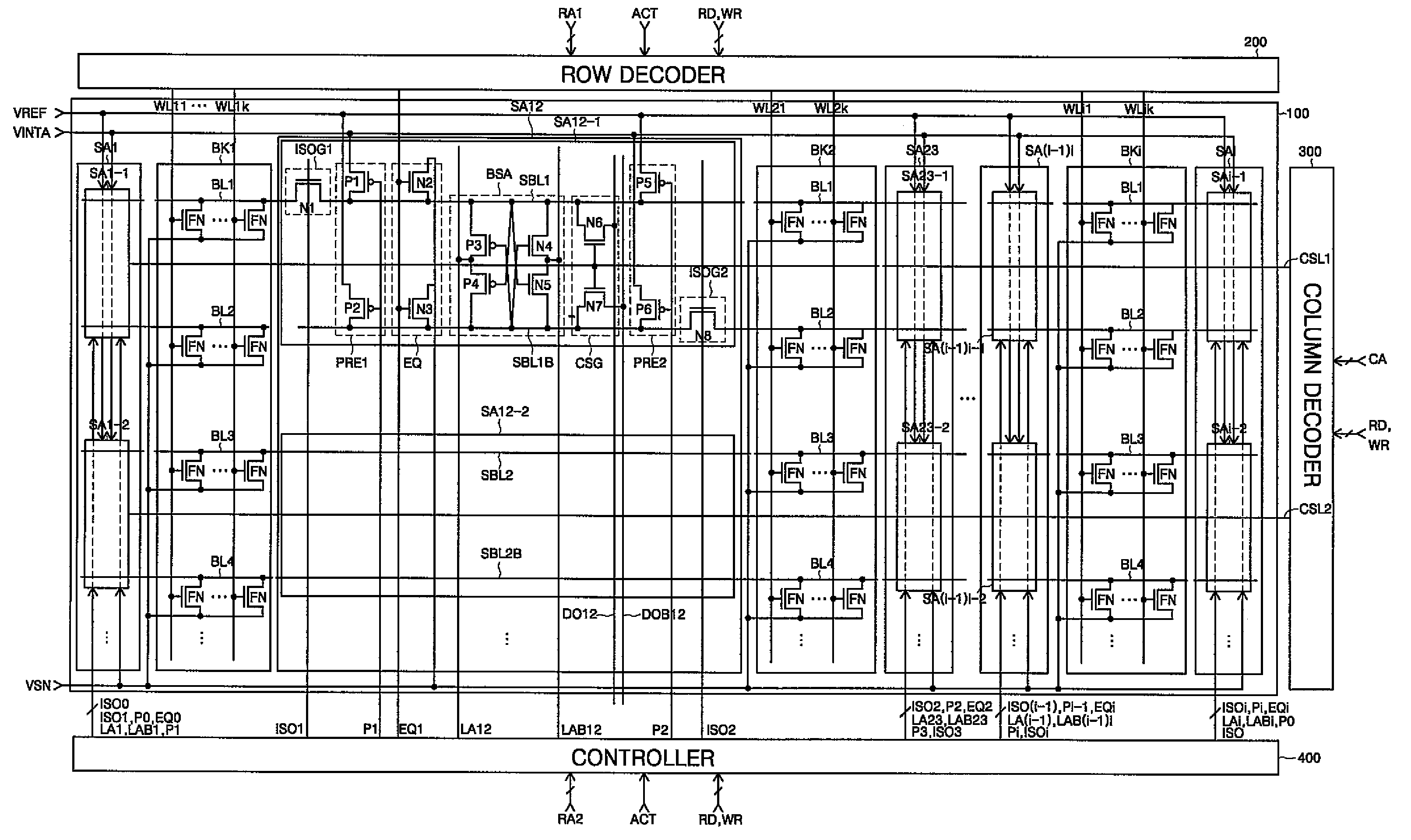
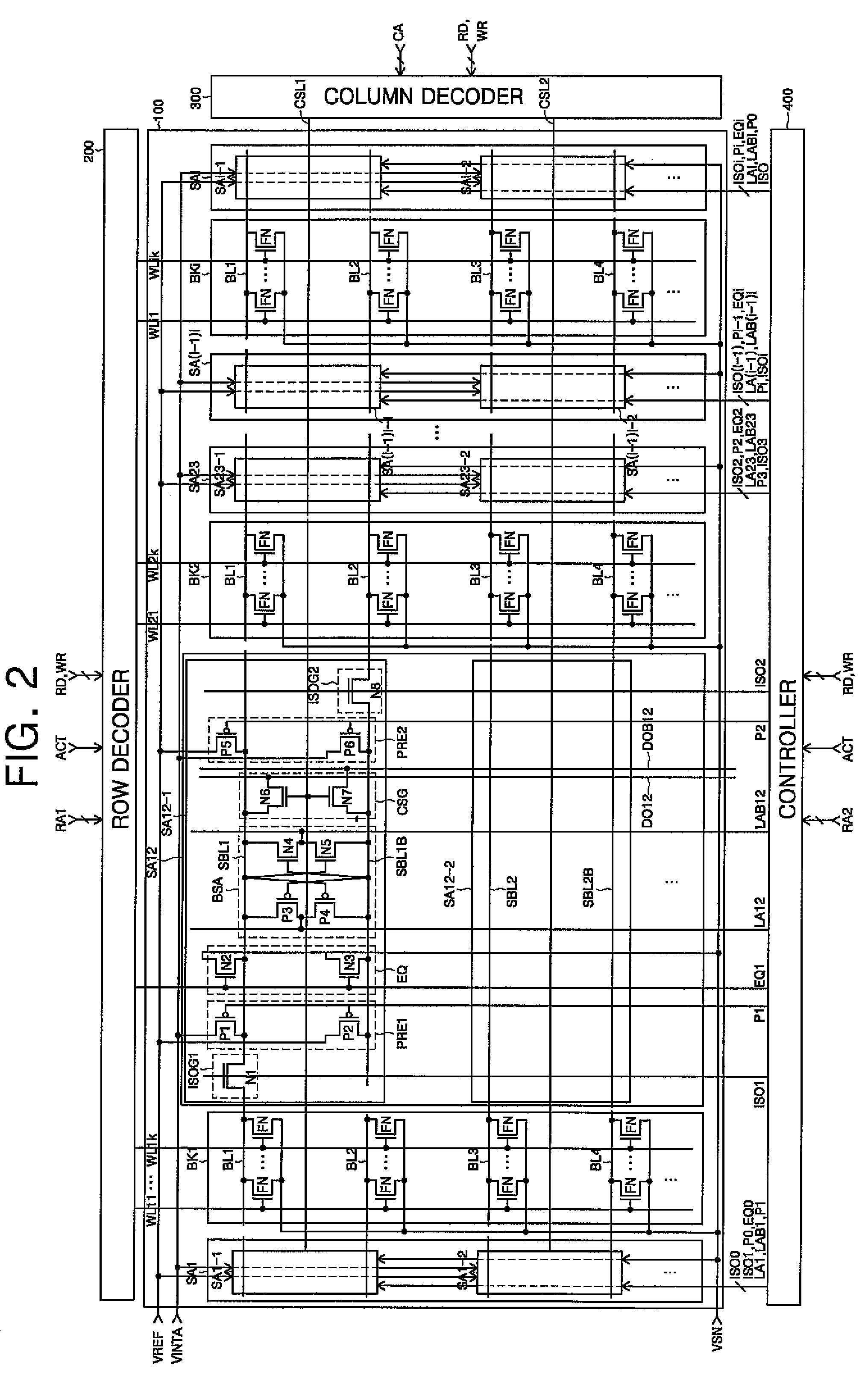
[0036]FIG. 2 is a circuit diagram illustrating an exemplary semiconductor memory device, which includes a memory cell with a floating body, according to an embodiment of the present invention. The semiconductor memory device of FIG. 2 includes a memory tell array 100, a row decoder 200, a column decod...


PUM


Abstract

A semiconductor memory device includes a memory cell array having first and second blocks, respectively including first and second memory cells with floating bodies. The first memory cell is connected between a first bit line and a source line, and the second memory cell is connected between a second bit line and the source line. A sense amplifier equalizes the sense bit line and the inverted sense bit line to be an equalization voltage during an equalization operation, pre-charges the sense bit line and the inverted sense bit line to first and second pre-charge voltages during a pre-charge operation, and amplifies a voltage difference between the sense bit line and the inverted sense bit line during read and write operations. The first pre-charge voltage is higher than the equalization voltage and the second pre-charge voltage is higher than the equalization voltage and lower than the first pre-charge voltage.

Description

CROSS-REFERENCE TO RELATED APPLICATION[0001]A claim of priority is made to Korean Patent Application No. 10-2006-0105838, filed Oct. 30, 2006, the subject matter of which is hereby incorporated herein by reference.BACKGROUND OF THE INVENTION[0002]1. Field of the Invention[0003]The present invention relates to a semiconductor memory device. More particularly, the present invention relates to a semiconductor memory device having a memory cell, including a floating body transistor, and a method of operating the same.[0004]2. Description of the Related Art[0005]A typical dynamic memory cell in a semiconductor memory device includes an access transistor and a corresponding data storage capacitor. Data “1” is stored when there is a charge in the capacitor, and data “0” is stored when there is no charge in the capacitor. However, the capacitor charge dissipates after a predetermined time lapses, and thus the capacitor needs to be periodically refreshed (re-stored). A semiconductor memory d...

Claims


Application Information

Patent Timeline
Patent Type & Authority Patents(United States)
IPC IPC(8): G11C11/24
CPCG11C11/4091G11C11/4094G11C2211/4016G11C5/14
Inventor KIM, DOO-GONPARK, DUK-HAKANG, MYOUNG-GON
Owner SAMSUNG ELECTRONICS CO LTD
Why Eureka
Try Eureka