Back-gate coupling voltage control oscillator

a voltage control and backgate technology, applied in the direction of oscillator, pulse technique, angle modulation details, etc., can solve the problems of increasing power consumption and increasing the difficulty of optimizing characteristics, so as to reduce the required circuit area, reduce power consumption and phase noise, and improve the effect of phase nois

Inactive Publication Date: 2009-06-09
NAT TAIWAN UNIV OF SCI & TECH
View PDF6 Cites 21 Cited by
  • Summary
  • Abstract
  • Description
  • Claims
  • Application Information

AI Technical Summary

Benefits of technology

[0015]The present invention is to provide a VCO, which is capable of improving the phase noise thereof and effectively reducing the required circuit area.
[0016]The present invention provides a VCO, which includes a VCO circuit and a back-gate coupling circuit. The VCO circuit includes at least a first transistor, a second transistor and a resonant cavity formed by inductors and capacitors, while the back-gate coupling circuit is formed by a plurality of capacitors and a plurality of resistors. In the embodiment of the present invention, the above-mentioned capacitor is coupled between the first transistor and the back-gate terminal of the second transistor to reduce the power consumption and the phase noise.
[0017]Since the present invention utilizes the back-gate coupling scheme, the usage area of the MOS transistors thereof and the power consumption of the circuit itself can be reduced. In addition, the use of small size MOS transistors generate less phase noise. Therefore, the present invention is capable of reducing the phase noise.

Problems solved by technology

Herein the phase noise of an OCR is a key factor affecting the quality of transmitting and receiving information and the reliability of an RF product.
Although the above-mentioned conventional schemes can improve the phase noise of a VCO, but the schemes also bring the new problems to the VCO that the circuit would occupy more area on a chip, increase power consumption and increase the difficulty of optimizing characteristics.

Method used


Image

  • Back-gate coupling voltage control oscillator
  • Back-gate coupling voltage control oscillator
  • Back-gate coupling voltage control oscillator

Examples


first embodiment

The First Embodiment

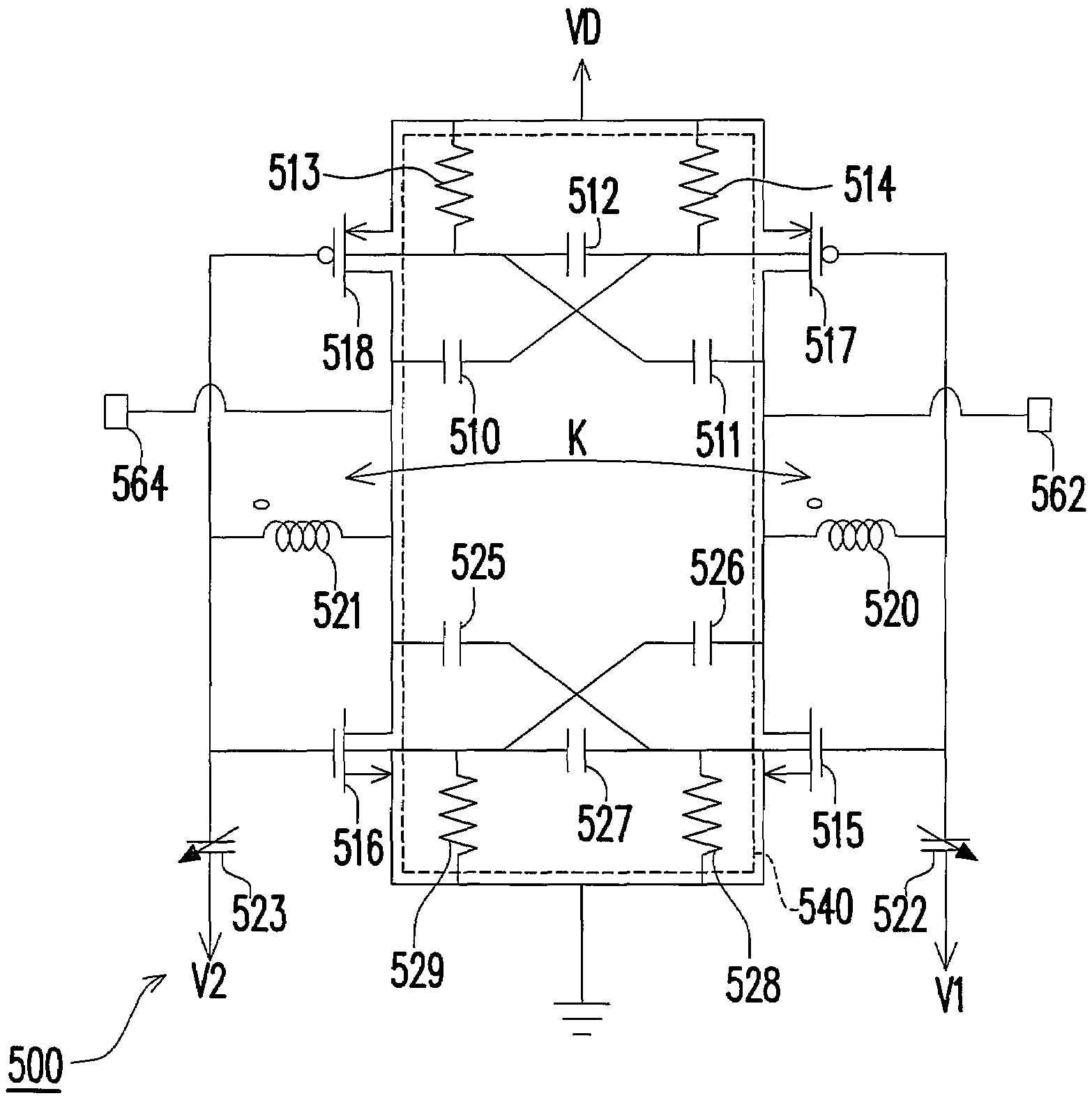
[0031]FIG. 5 is a schematic circuit drawing of a back-gate coupling VCO according to the first embodiment of the present invention. Referring to FIG. 5, the VCO 500 provided by the embodiment is a combination of two complementary single-terminal Colpitts oscillators, wherein the inductors in the two oscillators are coupled to each other to form a transformer-based differential VCO.

[0032]In FIG. 5, the transformer-based differential VCO 500 includes a differential MOS VCO circuit formed by PMOS transistors 517 and 518 and NMOS transistors 515 and 516 and a back-gate coupling circuit 540. In the embodiment, the source of the NMOS transistor 515 is grounded, the gate terminal thereof is coupled to a bias voltage VI via a varactor 522 and the drain terminal thereof is coupled to the output terminal 562. Similarly, the source of the NMOS transistor 516 is grounded, the gate terminal thereof is coupled to a bias voltage V2 via a varactor 523 and the drain terminal ther...

second embodiment

The Second Embodiment

[0039]FIG. 6 is a schematic circuit drawing of a back-gate coupling VCO according to the second embodiment of the present invention. Referring to FIG. 6, the VCO 600 provided by the embodiment is a differential oscillator composed of two PMOS single-terminal Colpitts oscillators, wherein the inductors in the two oscillators are coupled to each other and the NMOS transistors 610 and 611 are transconductance-coupled to each other, so as to form a transformer-based differential VCO.

[0040]The VCO 600 includes NMOS transistors 610, 611 and 618, PMOS transistors 612 and 613 and a back-gate coupling circuit 632. In the embodiment, the back-gate terminal and the source of the NMOS transistor 618 are grounded, the gate terminal thereof is coupled to a bias voltage V3 via and the drain terminal thereof is coupled to the source terminals of the NMOS transistors 610 and 611. The gate terminal of the NMOS transistor 610 is coupled to the drain terminal of the NMOS transistor...

third embodiment

The Third Embodiment

[0044]FIG. 7 is a schematic circuit drawing of a back-gate coupling VCO according to the third embodiment of the present invention. Referring to FIG. 7, the VCO 700 provided by the embodiment also includes NMOS transistors 710 and 711, a VCO circuit formed by PMOS transistors 712 and 713 and a back-gate coupling circuit 740.

[0045]In FIG. 7, the source terminal of the PMOS transistor 710 is grounded, the drain terminal thereof is coupled to an output terminal 762 and the gate terminal thereof is coupled to the gate terminal of the PMOS transistor 712. Similarly, the source terminal of the PMOS transistor 711 is grounded, the drain terminal thereof is coupled to an output terminal 764 and the gate terminal thereof is coupled to the gate terminal of the PMOS transistor 713.

[0046]The drain terminal of the PMOS transistor 712 is coupled to the output terminal 762, while the source terminal and the back-gate terminal thereof are coupled to a voltage source VD. Similarl...


PUM


Abstract

A voltage control oscillator (VCO) includes a VCO circuit and a back-gate coupling circuit, wherein the VCO circuit includes at least a first transistor, a second transistor and a resonant cavity formed by an inductor and a capacitor. The back-gate coupling circuit is formed by a plurality of capacitors and a plurality of resistors. In the embodiments of the present invention, the capacitors are coupled to the back-gate terminals of the first transistor and the second transistor, so as to reduce the power consumption and the phase noise of the VCO.

Description

CROSS-REFERENCE TO RELATED APPLICATION[0001]This application claims the priority benefit of Taiwan application serial no. 95138947, filed Oct. 23, 2006. All disclosure of the Taiwan application is incorporated herein by reference.BACKGROUND OF THE INVENTION[0002]1. Field of the Invention[0003]The present invention generally relates to a voltage control oscillator (VCO), and more particular, to a VCO including a back-gate coupling circuit.[0004]2. Description of Related Art[0005]Along with the rapid progress of radio frequency technology (RF technology), the demand on the RF products with high performance and extreme-low cost is increased. Herein the phase noise of an OCR is a key factor affecting the quality of transmitting and receiving information and the reliability of an RF product. Therefore, it has become the most important research topic to develop a VCO with low power-consumption and low phase noise.[0006]In terms of the differential LC-tank VCO which has been developed rece...

Claims


Application Information

Patent Timeline
Patent Type & Authority Patents(United States)
IPC IPC(8): H03B5/18
CPCH03B5/1228H03B5/1212H03B5/1296H03B5/124
Inventor JANG, SHENG-LYANGLEE, SHAO-HUACHUANG, YUN-HSUEHCHIU, CHUNG-CHING
Owner NAT TAIWAN UNIV OF SCI & TECH
Why Eureka
Try Eureka