Shared memory interface in a programmable logic device using partial reconfiguration

a technology of shared memory and programmable logic, which is applied in the direction of logic circuits, pulse techniques, electronic switching, etc., can solve the problems of limiting simulation performance and affecting performance in simulating a system requiring large amounts of data transfer

Active Publication Date: 2009-06-09
XILINX INC
View PDF2 Cites 71 Cited by
  • Summary
  • Abstract
  • Description
  • Claims
  • Application Information

AI Technical Summary

Problems solved by technology

The overhead associated with the data transfer between the HLMS and the hardware-based co-simulation platform may limit the performance for the simulation.
For example, performance may be severely impacted in simulating a system requiring large amounts of data transfer, such as real-time signal processing applications including video and image processing.

Method used


Image

  • Shared memory interface in a programmable logic device using partial reconfiguration
  • Shared memory interface in a programmable logic device using partial reconfiguration
  • Shared memory interface in a programmable logic device using partial reconfiguration

Examples


Embodiment Construction

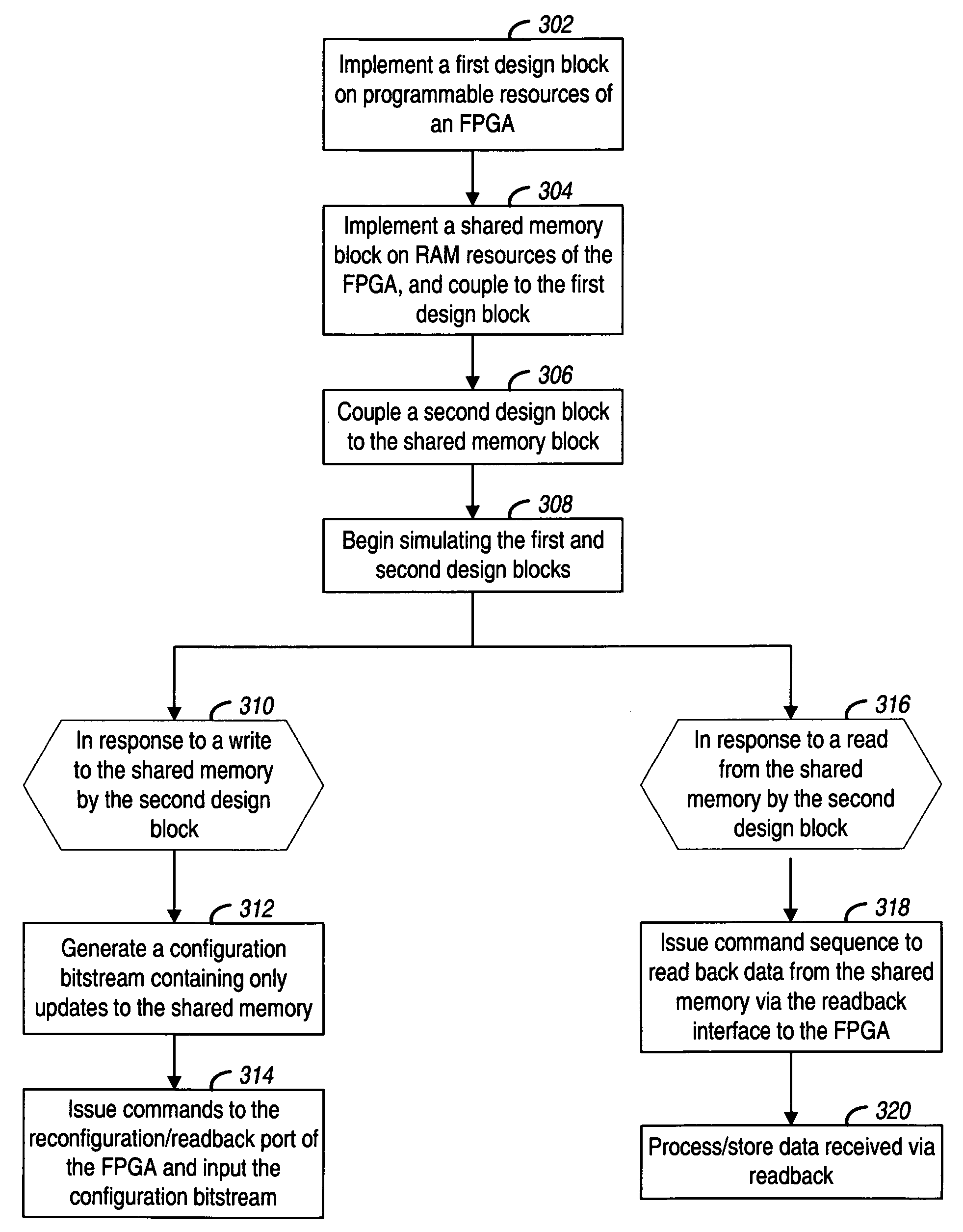
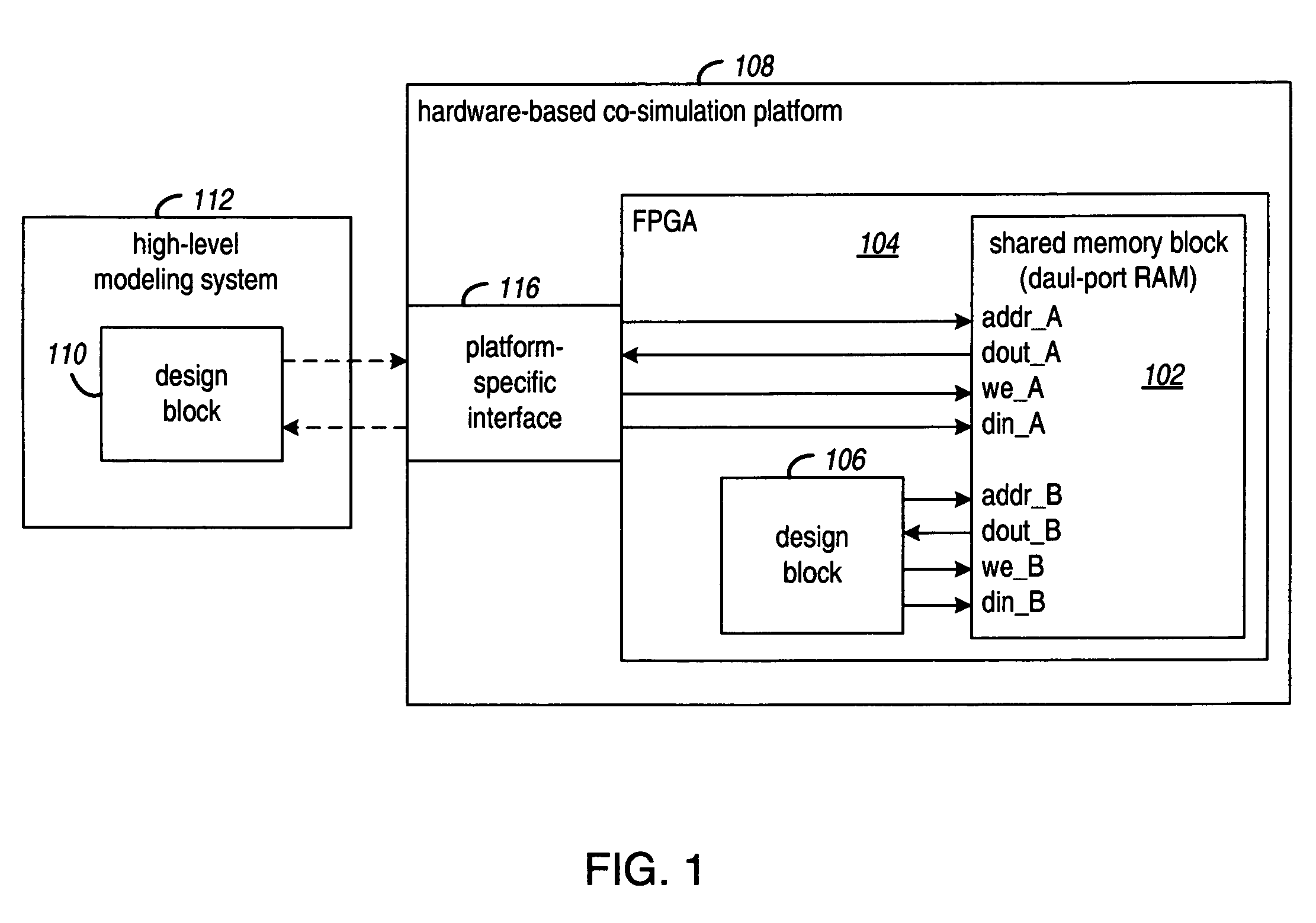
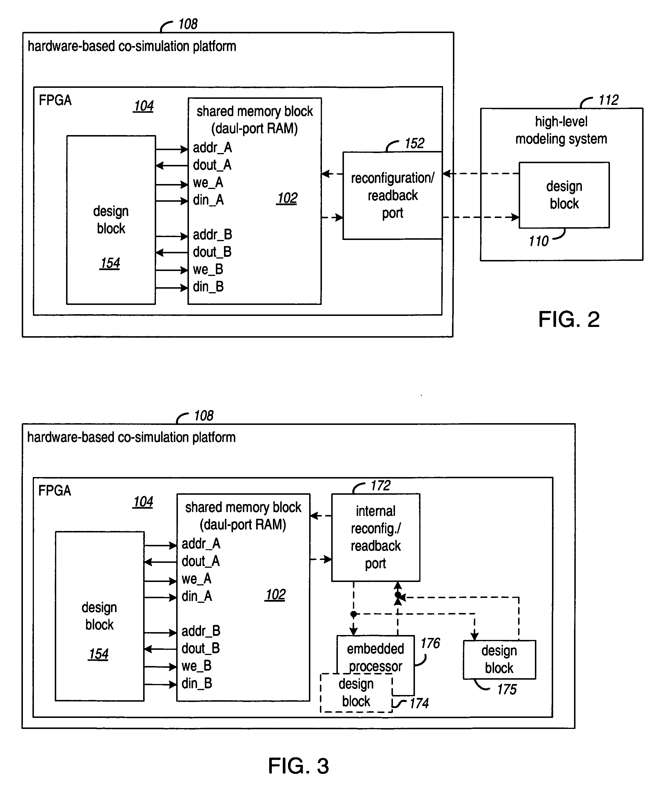
[0023]A shared memory block may be used to interface between a design block in an HLMS and a design block implemented on a hardware-based co-simulation platform. The shared memory block may span the software and hardware platforms, may be hosted solely on the software platform (e.g., a shared memory between two software processes), or implemented only on the hardware platform (e.g., a shared memory, such as a FIFO, between two portions of a circuit.) In one specific implementation, the shared memory block may be implemented on the hardware-based co-simulation platform as a dual port memory.

[0024]FIG. 1 is a block diagram that illustrates a shared memory block 102 implemented on a programmable logic device 104 for providing an interface between a design block 106 simulated on a reconfigurable hardware-based co-simulation platform 108 and a design block 110 simulated in a software-based system such as a high-level modeling system (HLMS) 112. In the example implementation the shared me...


PUM


Abstract

Partial reconfiguration of a programmable logic device is used in combination with a shared memory block for communicating between two blocks of an electronic circuit design. In one embodiment, a shared memory is implemented on RAM resources of a field programmable gate array (FPGA), and a first design block implemented in resources of the FPGA is coupled to the shared memory. A second design block is also coupled to the shared memory. In response to a write request by the second design block, a process determines the RAM resources of the FPGA that correspond to the shared memory address in the write request. A configuration bitstream is generated to include configuration data for partial reconfiguration of the FPGA with the data from the write request at the appropriate RAM resources. The FPGA is partially reconfigured with the configuration bitstream via a configuration port of the FPGA.

Description

FIELD OF THE INVENTION[0001]The present invention generally relates to a shared memory interface implemented in a programmable logic device (PLD).BACKGROUND[0002]During the process of developing a circuit design, the behavior of the design is simulated based on a specification of the circuit design. Simulating the design helps to verify correct behavior prior to physical implementation of the circuit. Wasted manufacturing costs due to faulty design may thereby be avoided.[0003]Numerous tools are available for preparing and simulating circuit designs including, for example, high-level modeling systems (HLMSs). Co-simulation may also be used when the design may be more efficiently simulated by simulating different parts of the design on different simulation platforms (“co-simulation platforms”).[0004]Example co-simulation platforms include both software-based and hardware-based systems. In a software-based system, a portion of the design is emulated with software running on a workstat...

Claims


Application Information

Patent Timeline
Patent Type & Authority Patents(United States)
IPC IPC(8): H03K17/693
CPCH03K19/17732H03K19/17756H03K19/1776
Inventor BALLAGH, JONATHAN B.MILNE, ROGER B.SHIRAZI, NABEELSTROOMER, JEFFREY D.
Owner XILINX INC
Why Eureka
Try Eureka