Reflection type display device and method with pixel electrodes having predetermined dimensions and relationships to each other as to gap width therebetween on both short and long sides and pitch of cubic corner cubes

a display device and pixel electrode technology, applied in non-linear optics, instruments, optics, etc., can solve the problems of reducing the aperture ratio, lowering applying this technique, etc., to improve the aperture ratio, improve the efficiency of light utilization, and stabilize the alignment of liquid crystals

Inactive Publication Date: 2009-06-23
SHARP KK
View PDF21 Cites 6 Cited by
  • Summary
  • Abstract
  • Description
  • Claims
  • Application Information

AI Technical Summary

Benefits of technology

[0018]In order to overcome the problems described above, preferred embodiments of the present invention provide a reflection-type LCD which realizes an improved aperture ratio and an improved efficiency of light utilization while maintaining a stable alignment in the liquid crystal.
[0031]According to the present invention, a reflective layer is provided as a separate element from the pixel electrodes, and therefore it is unnecessary to split the reflective layer into portions which are spaced apart so as to correspond to the pixels. Therefore, the area of the reflective layer can be increased, whereby the efficiency of light utilization can be improved. Moreover, since the patterning of the pixel electrodes can be performed irrespectively of the configuration of the protrusions and depressions of the reflective layer, an improvement in the aperture ratio can be obtained by reducing the gaps between pixel electrodes. Therefore, bright and high-contrast ratio images can be displayed.
[0032]Furthermore, the protrusions and depressions of the reflective layer are planarized, so that the orientation of the liquid crystal molecules can be stably controlled. Since the layer for realizing planarization (planarization layer) is not formed between the liquid crystal layer and the pixel electrodes, there is no voltage drop associated with the provision of the planarization layer.

Problems solved by technology

Firstly, the reflection electrodes 105 of the shape as shown in FIG. 1B are typically formed by patterning a concavo-convex metal film. However, it is difficult to perform a highly precise patterning for a concavo-convex metal film. In particular, when a metal film having a complicated surface configuration, e.g., a metal film having a corner cube array structure, it is difficult to form the reflection electrodes 105 in the designed manner, because the metal film is likely to be etched with dependence on the size and / or array pattern of the corner cubes. Therefore, it is difficult to reduce the interspaces between adjoining reflection electrodes 105, and thus the aperture ratio is decreased. Furthermore, since any light entering the gaps between reflection electrodes 105 is not reflected, the efficiency of light utilization is lowered, too. In answer to this problem, the Applicant has proposed in Japanese Laid-Open Patent Publication No. 2003-195788, supra, to perform a patterning of the reflection electrodes 105 in a manner to match the array pattern of the corner cubes, thus to reduce the interspaces between adjoining reflection electrodes 10; however, as the size of each corner cube becomes more minuscule, it becomes more difficult to apply this technique. In addition, design freedom of the reflection electrodes 105 is limited.
Secondly, the protrusions and depressions on the surface profile of the alignment film 118 of the rear substrate 109 make it difficult to realize a stable alignment in the liquid crystal layer 113. In the case where there is a large difference in levels between the depressions and the protrusions on the surface of the alignment film 118, the consequent variations in the thickness of the liquid crystal layer 113 may affect the displaying characteristics.
Although a retroreflection-type LCD is exemplified above, those reflection-type LCDs whose reflective layer is a reflection plate having diffuse reflection characteristics also have reflection electrodes which function both as a reflective layer and pixel electrodes, similarly to the structure shown in FIG. 1; therefore, such reflection-type LCDs also have problems similar to those described above.
However, a voltage drop is caused by the insulative film which is formed between the liquid crystal layer and the reflection electrodes, and therefore a high driving voltage is required.
However, it is difficult to perform a highly precise patterning for such a metal film.
Moreover, there is a problem in the case of performing a patterning utilizing protrusions and depressions, in that the design freedom of the reflection electrodes is limited.
Thus, it is difficult to enhance the aperture ratio and / or efficiency of light utilization by reducing the interspaces between reflection electrodes.
Furthermore, there is also a problem in that, since a liquid crystal layer is formed on a surface having protrusions and depressions, it is difficult to stably control the alignment in the liquid crystal layer.

Method used


Image

  • Reflection type display device and method with pixel electrodes having predetermined dimensions and relationships to each other as to gap width therebetween on both short and long sides and pitch of cubic corner cubes
  • Reflection type display device and method with pixel electrodes having predetermined dimensions and relationships to each other as to gap width therebetween on both short and long sides and pitch of cubic corner cubes
  • Reflection type display device and method with pixel electrodes having predetermined dimensions and relationships to each other as to gap width therebetween on both short and long sides and pitch of cubic corner cubes

Examples


first embodiment

[0073]Hereinafter, a first embodiment of the reflection-type LCD according to the present invention will be described.

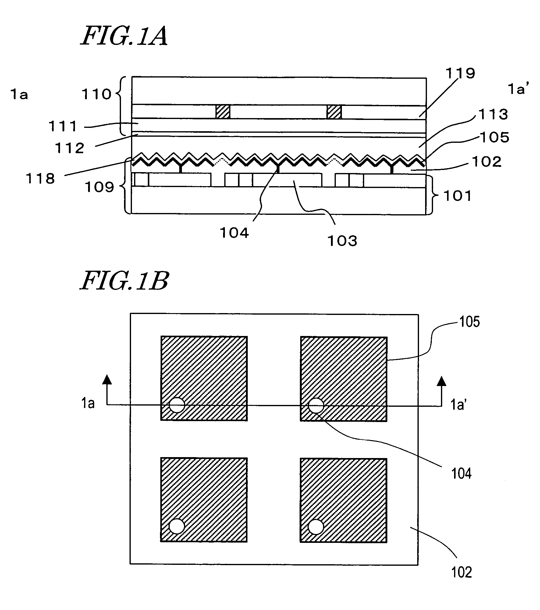
[0074]FIG. 4A is a plan view showing the structure of a rear substrate (TFT-side substrate) 300 in the reflection-type LCD of the present embodiment. FIG. 4B is a cross-sectional view taken along line 4b-4b′ in the plan view of FIG. 4A.

[0075]The rear substrate 300 includes the following elements which are disposed in this order on a substrate 301: an active switch layer 301s; an insulating layer 307; a reflective layer 308; a planarization resin layer 309; and pixel electrodes 310. In the present embodiment, the active switch layer 301s includes a plurality of thin film transistors 301t. Each thin film transistor 301t includes, for example, a gate electrode 302, a gate insulative film 303 covering the gate electrode 302, a semiconductor layer 304 formed on the gate insulative film 303, a source line and source bus 305, and a drain electrode 306. Although the thin fil...

second embodiment

[0155]Hereinafter, a reflection-type display device according to a second embodiment of the present invention will be described.

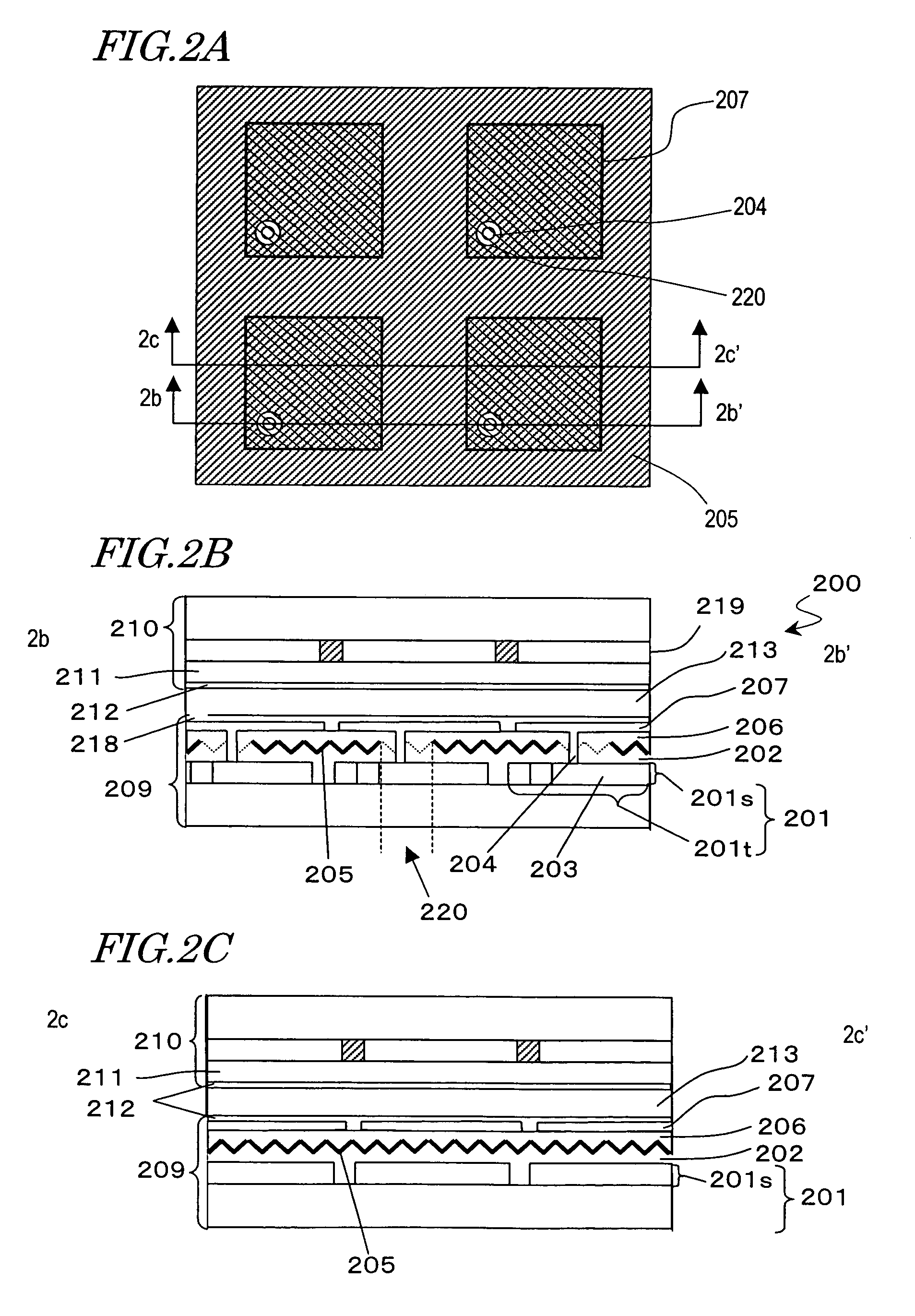
[0156]FIG. 13A is a plan view showing the structure of a rear substrate (TFT-side substrate) 400 in the reflection-type LCD of the present embodiment. FIG. 13B is a cross-sectional view taken along line 13b-13b′ in the plan view of FIG. 13A.

[0157]The rear substrate 400 has a similar structure to that of the rear substrate 300 which has been described with reference to FIGS. 4A and 4B. However, the rear substrate 400 differs from the rear substrate 300 in that the insulating layer 407 has a diffuse reflection configuration rather than a retroreflective configuration, and the reflective layer 408 has scatter reflection characteristics rather than retroreflection characteristics.

[0158]The rear substrate 400 of the present embodiment can be formed by a method described below, for example.

[0159]First, a TFT substrate is formed by using a method similar to that w...


PUM

PropertyMeasurementUnit
diameteraaaaaaaaaa
diameteraaaaaaaaaa
gap widthaaaaaaaaaa

Abstract

A reflection-type display device 200 includes: an active switch layer 201s including a plurality of switching elements 201t; a plurality of pixel electrodes 207 each connected to a corresponding one of the plurality of switching elements 201t; a reflective layer 205 formed between the active switch layer 201s and the plurality of pixel electrodes 207; and a modulation layer 213 provided at a side of the pixel electrodes 207 facing a viewer, the modulation layer 213 being capable of switching between a first state and a second state of respectively different optical characteristics. The reflective layer 205 is connected to neither the plurality of switching elements 201t nor the plurality of pixel electrodes 207.

Description

BACKGROUND OF THE INVENTION[0001]1. Field of the Invention[0002]The present invention relates to a reflection-type display device and a method for producing the same.[0003]2. Description of the Related Art[0004]Liquid crystal display device (hereinafter “LCDs”) of a reflection type, which perform display by utilizing ambient light as a light source, have been known. Since reflection-type LCDs do not require a backlight as do transmission-type LCDs, reflection-type LCDs are suitably used for various devices which must have a light weight and a thin thickness. In particular, reflection-type LCDs of an active matrix driving type, in which a switching element is provided corresponding to each pixel, are capable of performing display with a high resolution and high quality.[0005]In order to further improve the display performance of a reflection-type LCD, a retroreflection-type LCD which includes a retroreflection plate as a reflective layer for reflecting ambient light is proposed. As u...

Claims


Application Information

Patent Timeline
Patent Type & Authority Patents(United States)
IPC IPC(8): G02F1/1335G02F1/1362
CPCG02F1/133553G02F1/136227G02F1/1335
Inventor FUJIWARA, SAYURISAWAYAMA, YUTAKAMINOURA, KIYOSHIKANBE, MAKOTO
Owner SHARP KK
Why Eureka
Try Eureka