Detection of resonator motion using piezoresistive signal downmixing

a piezoresistive signal and motion detection technology, applied in the field of microelectromechanical systems, can solve the problems of difficult to achieve high quality, frequency-dependent signal attenuation at mhz frequencies, and significant limitation of attenuation to achieve the effect of high quality

Active Publication Date: 2009-06-30
CALIFORNIA INST OF TECH
View PDF39 Cites 30 Cited by
  • Summary
  • Abstract
  • Description
  • Claims
  • Application Information

AI Technical Summary

Problems solved by technology

However, it has proved difficult to achieve high quality results using the piezoresistive technique in NEMS due to the intrinsically high resistances (5-100 kΩ) of these devices, which leads to frequency-dependent signal attenuation at MHz frequencies if direct current detection is used.
Such attenuation poses a significant limitation to this method as the resonance frequencies are increased to the high-frequency range and beyond.
However, this may be difficult if the impedance mismatch ratio is greater than 100 and impractical if the same detection setup is to be used with many devices of different frequencies.

Method used


Image

  • Detection of resonator motion using piezoresistive signal downmixing
  • Detection of resonator motion using piezoresistive signal downmixing
  • Detection of resonator motion using piezoresistive signal downmixing

Examples


first embodiment

1. First Embodiment

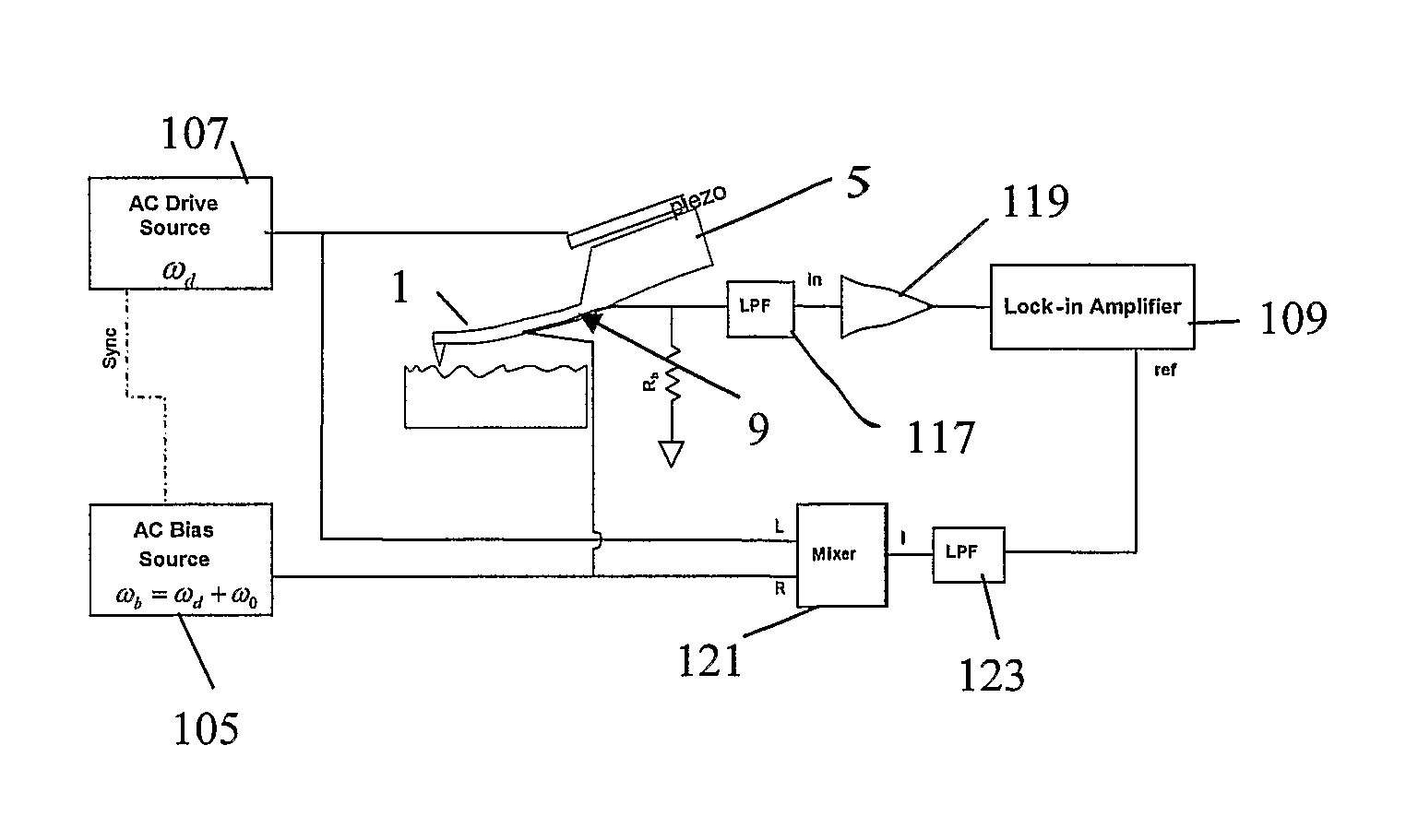
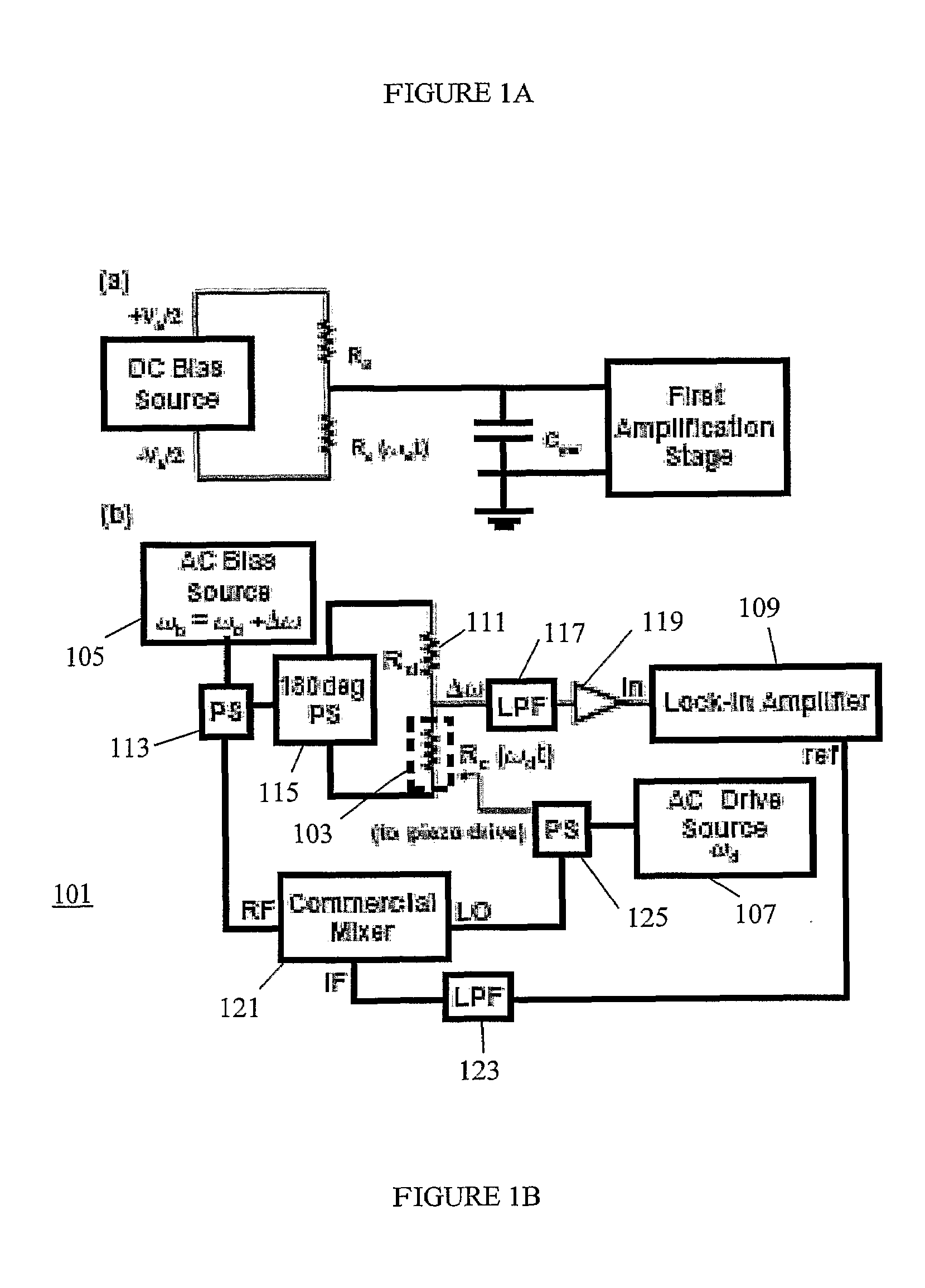
[0028]In a first embodiment of the invention, the present inventors have developed a system and method for measuring RF-range resonance properties of nano- or micro-mechanical devices which comprise entire or parts of micro- or nano-electro-mechanical systems (MEMS and NEMS, respectively), with integrated piezoresistive strain detectors serving as signal downmixers. Preferably but not necessarily, the piezoresistive elements comprise thin film elements and the technique takes advantage of the high strain sensitivity of thin film piezoresistors, while overcoming the problem of RF signal attenuation due to a high source impedance. The technique also reduces the effect of the cross-talk between the detector and actuator circuits. The method also allows a way to circumvent the problem of impedance mismatch and extends the usability of low-frequency, high-input-impedance preamplifiers and other equipment.

[0029]In one aspect of the first embodiment, the method includes ...

first example

A. First Example of First Embodiment

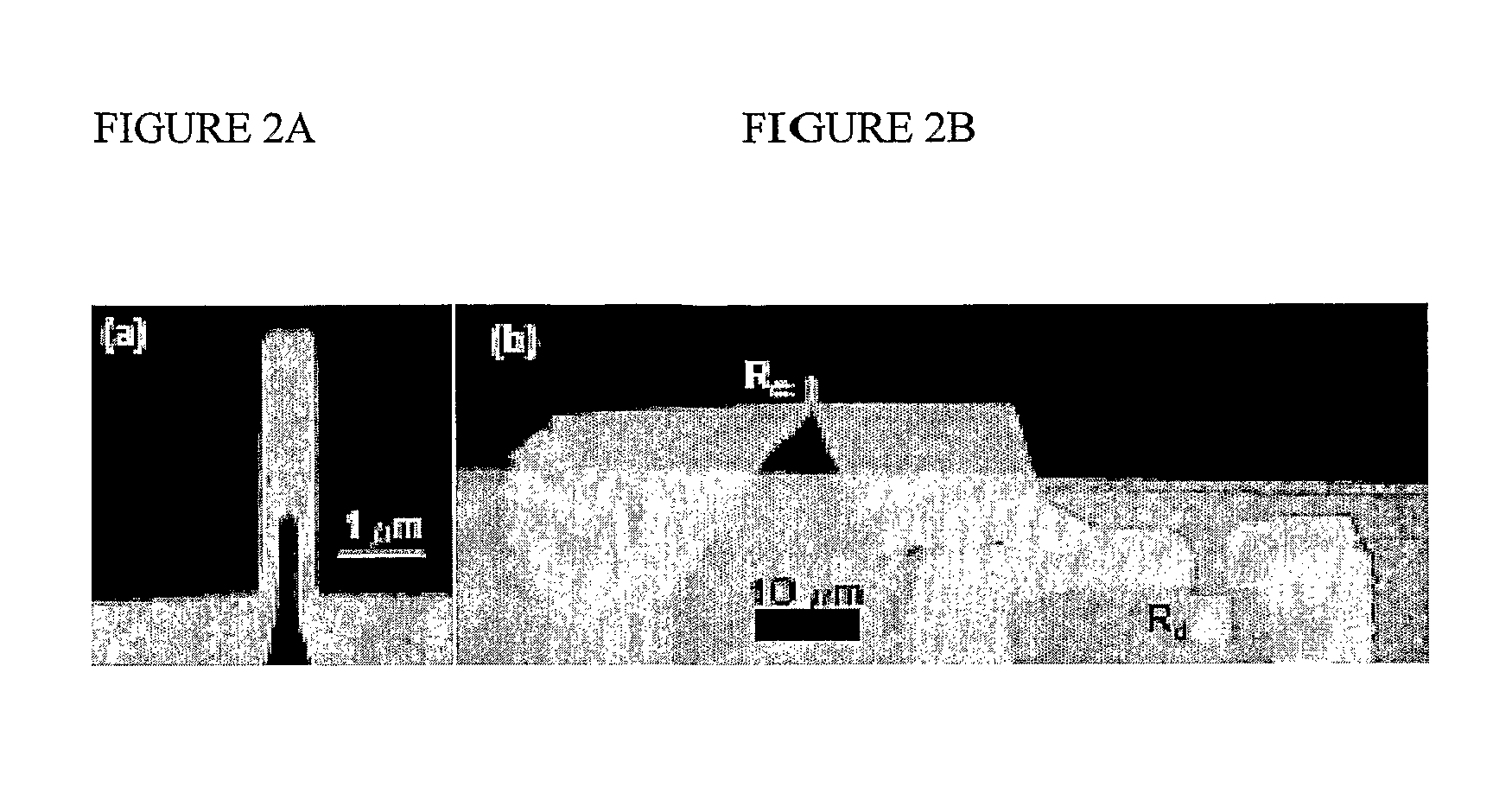
[0044]In a first example of the first embodiment, the downmixing scheme is tested using high-frequency piezoresistive cantilevers as the NEMS device 103. The cantilevers are fabricated from silicon-on-insulator (SOI) wafers, where the top Si layer consists of 80 nm Si plus a 30 nm layer of boron-doped p-Si to act as the piezoresistive strain sensor (i.e., a semiconductor piezoresistive film). The cantilevers were fabricated in a manner similar to that of described in J. A. Harley and T. W. Kenny, Appl. Phys. Lett. 75, 289 (1999), where a backside KOH etch suspends the top Si layer as a membrane, and a combination of electron beam lithography, liftoff, and fluorine / chlorine-based plasma etching steps forms the cantilever from the membrane. A typical cantilever is shown in FIG. 2A. Cantilever lengths ranged between about 2-3 μm and widths were approximately 700 nm. For example, the exemplary cantilever shown in FIG. 2A is 3.2 microns long, 700 nm wi...

second embodiment

2. Second Embodiment

[0064]In a second embodiment of the invention, a method of making nanoscale scanning probes is described. It should be noted that the method of the second embodiment may be used to make the resonator of the first embodiment. However, the resonator of the first embodiment may also be made by any other suitable method. Furthermore, the method of the second embodiment may be used to make a probe that is not used in the system and method of the first embodiment. Still further, while a cantilever shaped scanning probe is described, other resonators and sensor / imaging devices described above with respect to the first embodiment can be made instead.

[0065]Preferably, the probes of the second embodiment are used in NEMS adapted for scanning probe microscopy of biological samples. These probes preferably, but not necessarily fall into nanoscale size regime described above. For example, the thickness of the cantilever can be as thin as 30 nm, such as 30 nm to 150 nm. The wi...


PUM


Abstract

A system containing a micro-mechanical or nano-mechanical device and a method of operating the same is provided. The device includes a resonator and a piezoresistive element connected to the resonator. The method includes AC biasing the piezoresistive element at a first frequency, driving the resonator at a second frequency different from the first frequency, and detecting a mechanical response of the resonator at one or both of a difference frequency and a sum frequency of the first and second frequencies.

Description

CROSS-REFERENCE TO RELATED APPLICATIONS[0001]This application is a continuation-in-part of U.S. application Ser. No. 11 / 010,578 filed Dec. 14, 2004. This application also claims benefit of priority of both U.S. Provisional Application Ser. No. 60 / 562,652, filed Apr. 15, 2004, and U.S. Provisional Application Ser. No. 60 / 547,168, which was assigned a filing date of Feb. 25, 2004. All of the above mentioned applications are incorporated herein by reference in their entirety.STATEMENT REGARDING FEDERALLY SPONSORED RESEARCH OR DEVELOPMENT[0002]The U.S. Government may have certain rights in this invention pursuant to grant number ECS-0O89061 from the NSF and grant numbers DSO-MOSAIC N00014-02-1-0602 and MTO / SPAWAR N66001-02-1-8914 from DARPA.BACKGROUND OF THE INVENTION[0003]1. Field of the Invention[0004]This invention is related to micro-electro-mechanical systems (MEMS) and nano-electro-mechanical systems (NEMS).[0005]2. Description of the Prior Art[0006]The field of microelectromechan...

Claims


Application Information

Patent Timeline
Patent Type & Authority Patents(United States)
IPC IPC(8): G01B7/16
CPCB82Y35/00G01Q20/04
Inventor BARGATIN, IGORMYERS, EDWARD B.LI, MOARLETT, JESSICAGUDLEWSKI, BENJAMINROUKES, MICHAEL L.YOUNG, DARRON K.TANG, HONG X.
Owner CALIFORNIA INST OF TECH
Why Eureka
Try Eureka