Solid image capturing element for power saving at output section and manufacturing method for the same

Active Publication Date: 2009-07-07
SEMICON COMPONENTS IND LLC
View PDF15 Cites 0 Cited by
  • Summary
  • Abstract
  • Description
  • Claims
  • Application Information

AI Technical Summary

Benefits of technology

[0020]In recent years, many small and light-weight devices including a CCD solid image capturing element, such as digital cameras and portable phones with an image capturing function, have been developed and introduced into the marketplace. Because the battery used in such small, light-weight devices is generally small, reduction of power consumption is desired. Meanwhile, a CCD solid image capturing element requires a relatively large amount of current for driving an output amplifier and therefore consumes a relatively large power. For compensation for this large power consumption, a power voltage VDD to be applied to the output amplifier is reduced so that power consumption by the CCD solid image capturing element or the entirety of the image capturing device is reduced.

Problems solved by technology

Meanwhile, a CCD solid image capturing element requires a relatively large amount of current for driving an output amplifier and therefore consumes a relatively large power.
However, reduction of the applied power voltage VDD may lead to malfunction of the transistor of the output amplifier, which receives, at its drain, a power voltage VDD, and outputs, via its source, an amplified output.
For this reason, reduction of power consumption of a CCD solid image capturing element or the entirety of an image capturing element has remained an unsolved problem.

Method used


Image

  • Solid image capturing element for power saving at output section and manufacturing method for the same
  • Solid image capturing element for power saving at output section and manufacturing method for the same
  • Solid image capturing element for power saving at output section and manufacturing method for the same

Examples


Embodiment Construction

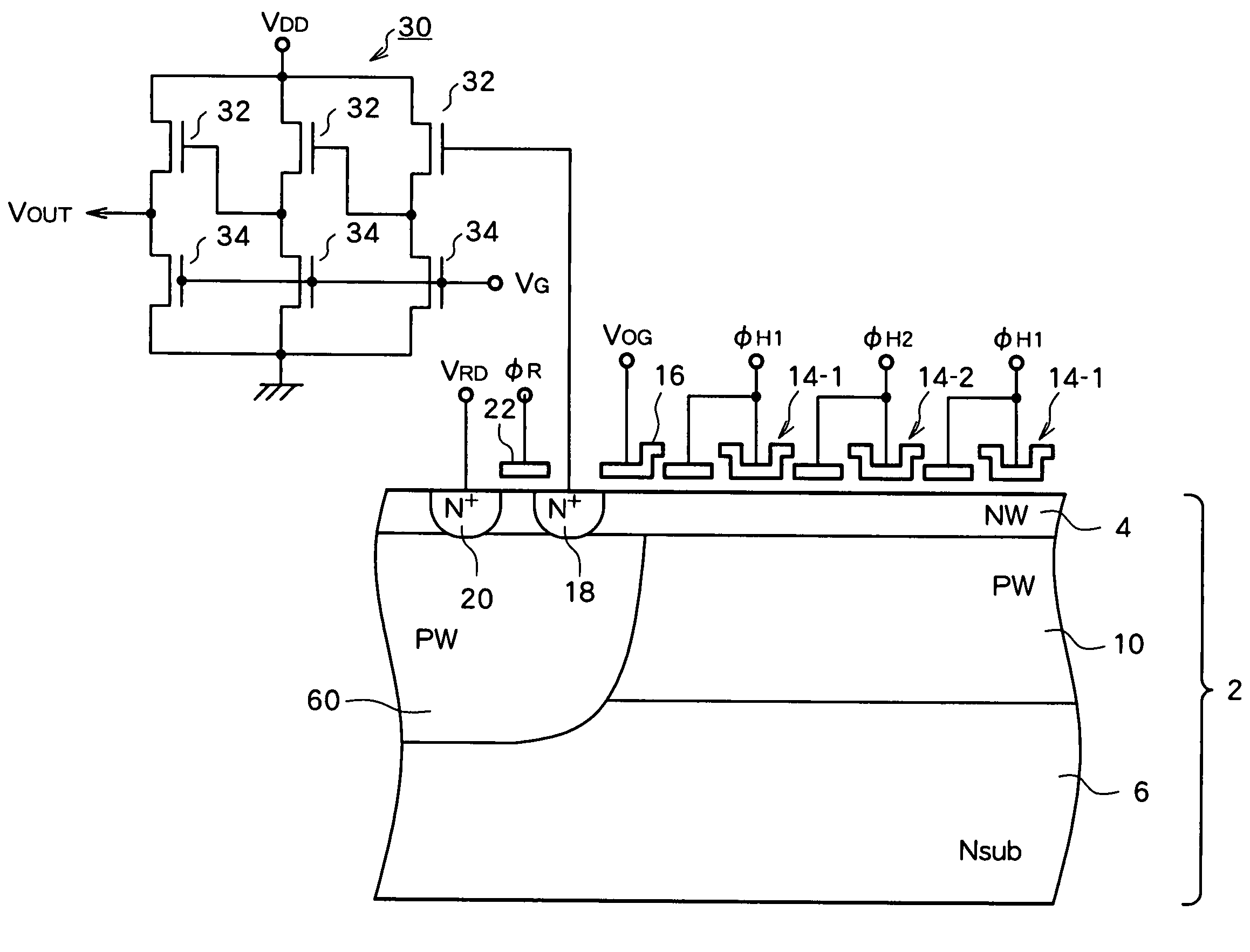
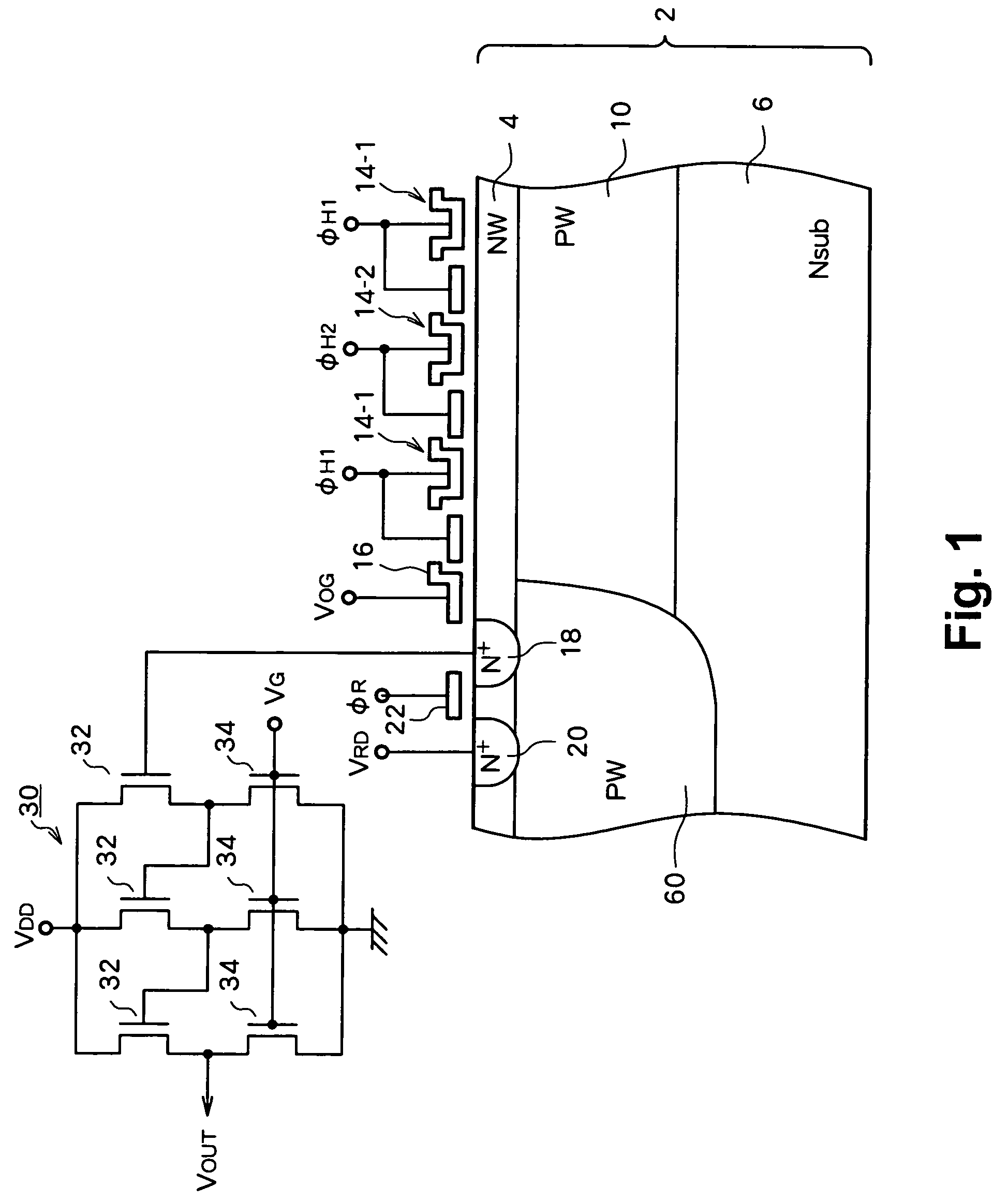
[0032]In the following, a preferred embodiment of the present invention will be described with reference to the accompanied drawings. In the following description, a CCD solid image capturing element using a frame transfer method will be referred to. The structure of a CCD solid image capturing element using a frame transfer method is schematically shown in FIG. 4, which is incorporated in the following description.

[0033]As described above, a CCD solid image capturing element using a frame transfer method comprises an image capturing section i, a storage section s, a horizontal transfer section h, and an output section d. The image capturing section i comprises a plurality of shift registers, vertically extending in the drawing, respectively arranged in parallel, in which each bit in each shift register forms photo diffusion and constitutes a light receiving pixel. The storage section s comprises a plurality of light-shielded shift registers continuing from the respective shift regi...


PUM


Abstract

A solid image capturing element comprising a plurality of vertical shift registers arranged to each correspond to a column of a plurality of light receiving pixels in a matrix arrangement, a horizontal shift register provided on an output side of the plurality of vertical shift registers, and an output section provided on an output side of the horizontal shift register. In this solid image capturing element, a reverse conductive semiconductor region is formed over one major surface of one conductive semiconductor substrate, the plurality of light receiving pixels, the plurality of vertical shift registers, the horizontal shift register, and the output section are formed in the semiconductor region, and a portion of the semiconductor region where the output section is formed has a higher dopant concentration than the portion of the semiconductor region where the horizontal shift register is formed.

Description

BACKGROUND OF THE INVENTION[0001]1. Field of the Invention[0002]The present invention relates to a CCD solid image capturing element and a method for manufacturing the same. In particular, the present invention relates to suppression of power consumption in an output section.[0003]2. Description of the Related Art[0004]FIG. 4 schematically shows a structure of a CCD solid image capturing element using a frame transfer method. Specifically, a CCD solid image capturing element using a frame transfer method comprises an image capturing section i, a storage section s, a horizontal transfer section h, and an output section d.[0005]The image capturing section i generates information charges in a two-dimensional array and transfers the charges at a high speed to the storage section s. The information charges are stored in the storage section s and also transferred to the subsequent horizontal transfer section h for every pixel row. The information charges are then transferred to the output...

Claims


Application Information

Patent Timeline
IPC IPC(8): H01L29/762H01L21/339H01L27/148H04N5/335H04N5/369H04N5/3725H04N5/378
CPCH01L27/14812Y10S257/912H01L27/148
Inventor OKADA, YOSHIHIROOTSURU, YUZO
Owner SEMICON COMPONENTS IND LLC
Why Eureka
Try Eureka