Low supply voltage bandgap system

a low-voltage bandgap and low-voltage technology, applied in the field of integrated circuits, can solve the problems of inability to adapt to cmos technology, limited maximum vpp, and inability to design voltage/current reference circuits, etc., to achieve precise level detection control and accurate dram wl voltage operation.

Inactive Publication Date: 2009-07-07
TAIWAN SEMICON MFG CO LTD
View PDF3 Cites 2 Cited by
  • Summary
  • Abstract
  • Description
  • Claims
  • Application Information

AI Technical Summary

Benefits of technology

[0006]An advantage of an illustrative embodiment of the present invention is that the system may be a low supply voltage integrated circuit with a logic process core voltage of one volt or less. A further advantage of an illustrative embodiment of the present invention is to prevent system feedback self-lock problems, in that the initial Vpp rough voltage level is provided by a simple control detector.

Problems solved by technology

However, due to reliability concerns, the maximum Vpp is limited due to the maximum allowable electric field across the gate oxide of the transfer transistor.
With steadily decreasing power supply voltages in CMOS technologies, the design of voltage / current references becomes more difficult.
The traditional voltage summing bandgap reference circuit is not suited for a CMOS technology with a maximum supply voltage of 1.0V or less.
This causes bandgap circuitry to fail.

Method used


Image

  • Low supply voltage bandgap system
  • Low supply voltage bandgap system
  • Low supply voltage bandgap system

Examples


Embodiment Construction

[0016]The making and using of the presently preferred embodiments are discussed in detail below. It should be appreciated, however, that the present invention provides many applicable inventive concepts that can be embodied in a wide variety of specific contexts. The specific embodiments discussed are merely illustrative of specific ways to make and use the invention, and do not limit the scope of the invention.

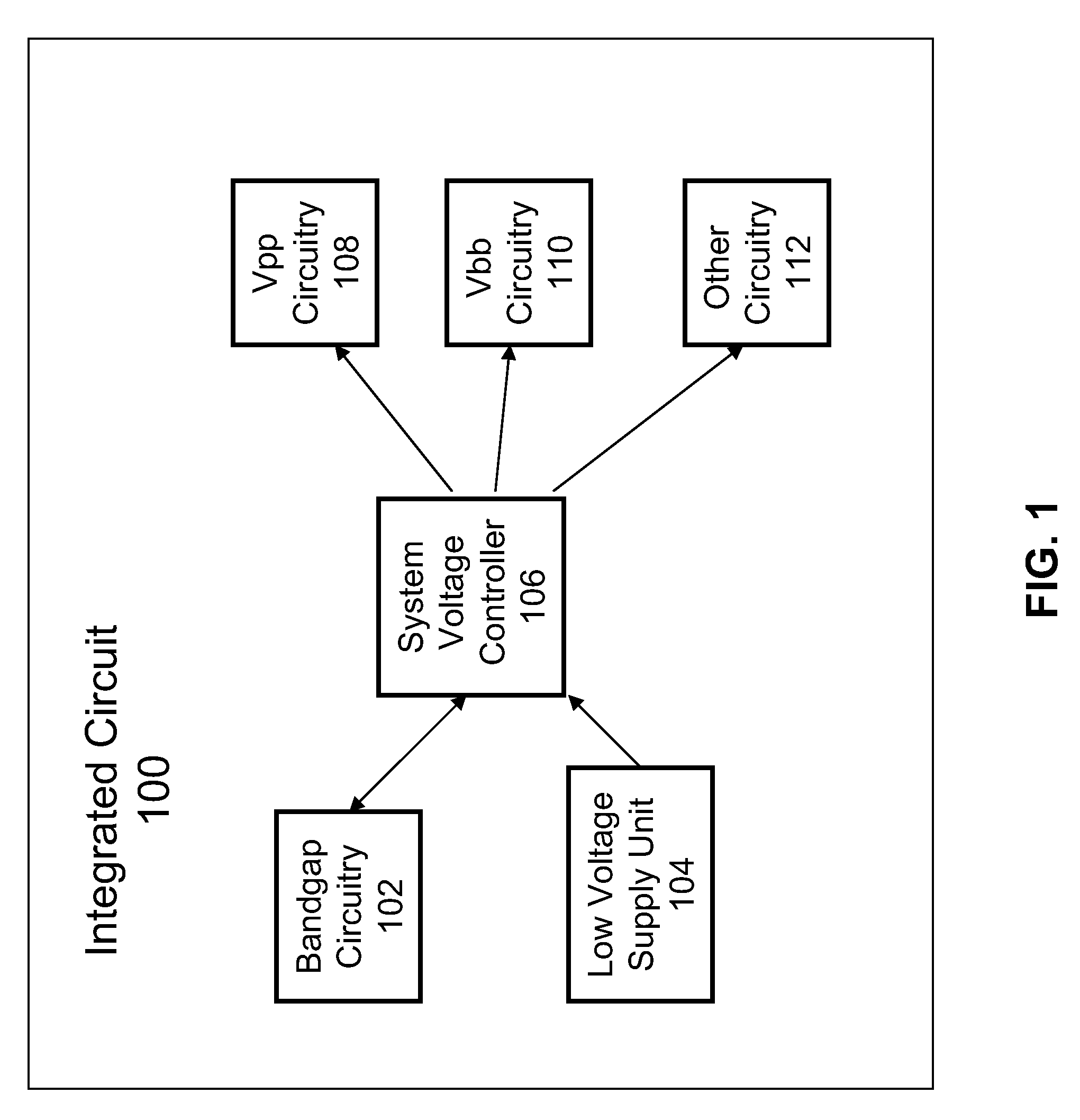
[0017]The present invention will be described with respect to preferred embodiments in a specific context, namely an eDRAM system, which may have a logic process core voltage of one volt or below. The invention may also be applied, however, to other integrated circuits with supply voltages lower than the operational voltage for a bandgap circuit.

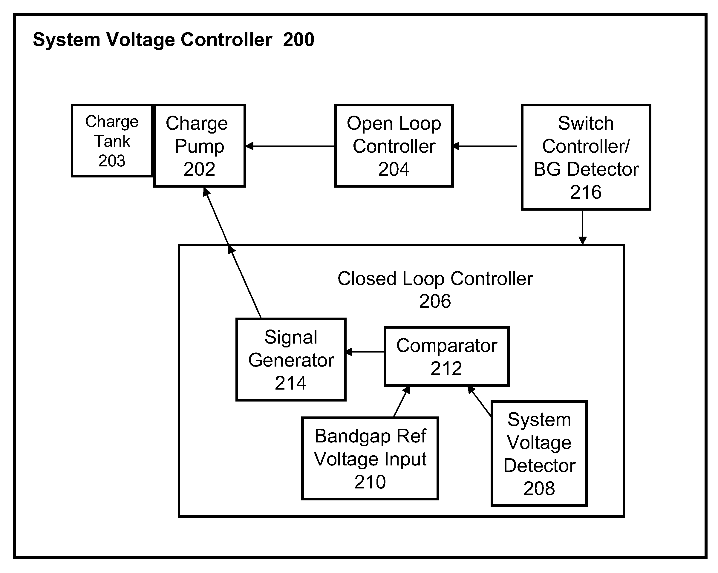
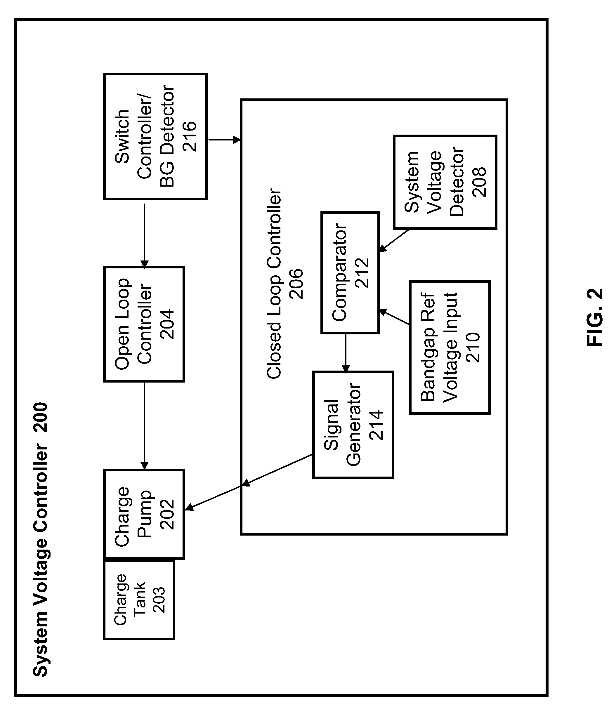
[0018]An example of an illustrative embodiment of the inventive system is implemented in an eDRAM cell. The embodiment allows bandgap circuitry to function on a low boosted wordline voltage (Vpp) integrated circuit, and for using the ...


PUM


Abstract

A system and a method is disclosed for allowing bandgap circuitry to function on a low supply voltage integrated circuit, and for using the reference voltage (Vbg) generated by the bandgap circuitry to enable a reference voltage to control system voltage. An illustrative embodiment comprises a charge pump to raise a supply voltage to a system voltage, and an open loop controller, which provides a first signal to activate the charge pump, enabling a bandgap circuit, which outputs a bandgap voltage reference. Further, the system comprises a closed loop controller, which regulates the system voltage by comparing the system voltage to the bandgap reference voltage. Upon the system voltage falling below a target voltage, the closed loop controller provides a second signal to activate the charge pump. Additionally the system comprises a switch controller, which selects the closed loop controller upon sensing the bandgap circuit is active.

Description

TECHNICAL FIELD[0001]The present invention relates generally to an integrated circuit, and more particularly to a system and a method for allowing bandgap circuitry to provide a reference voltage for a low supply voltage integrated circuit.BACKGROUND[0002]In conventional DRAM arrays, information is stored in a given DRAM cell by driving a wordline (WL) appropriately to activate a transfer transistor, and thereby transfer charge into the cell capacitor. In general, the retention time of the cell, and the performance of the cell, increases with the amount of charge transferred to the cell. The transfer transistor of a given cell is activated for transferring charge into the cell by application of a voltage Vpp to the wordline, and the transfer transistor is switched off by application of a voltage wordline low (WLL) to the wordline.[0003]In order to transfer the maximum possible charge to the cell, Vpp must be greater than the threshold voltage Vt of the transfer transistor. Therefore...

Claims


Application Information

Patent Timeline
Patent Type & Authority Patents(United States)
IPC IPC(8): G05F3/16
CPCG05F3/30
Inventor HSU, KUOYUAN PETERLEN, MAOFENG
Owner TAIWAN SEMICON MFG CO LTD
Why Eureka
Try Eureka