Light emitting element and method of making same
a technology of light-emitting elements and light-emitting elements, which is applied in the direction of basic electric elements, semiconductor devices, electrical equipment, etc., can solve the problems of limited light extraction efficiency, insufficient light extraction efficiency, and low external radiation efficiency of emitted light, and achieves enhanced external radiation efficiency and high optical absorption coefficient
- Summary
- Abstract
- Description
- Claims
- Application Information
AI Technical Summary
Benefits of technology
Problems solved by technology
Method used
Image

Examples
third embodiment
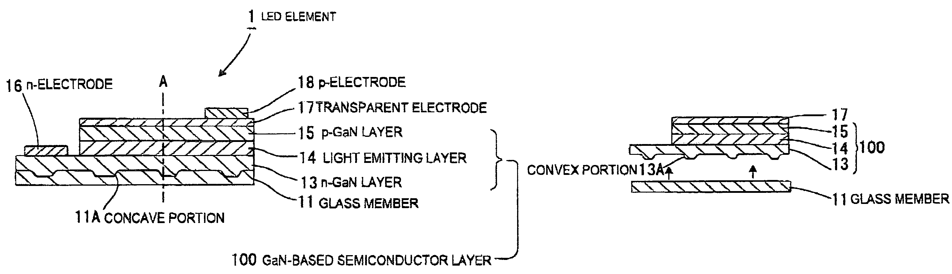
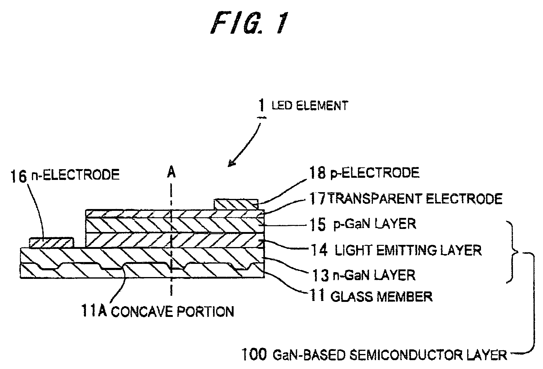
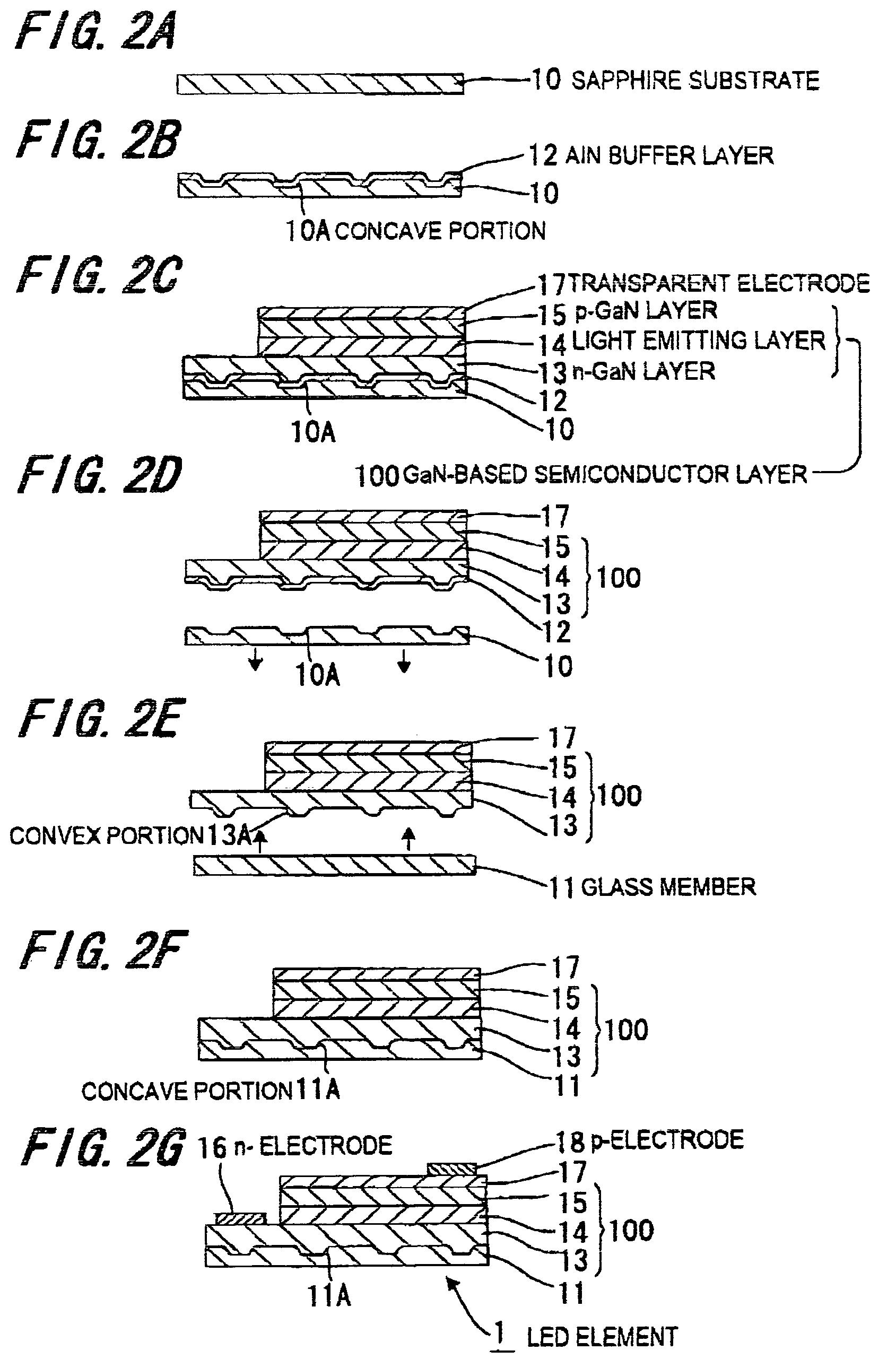
(Composition of LED Element 1)
[0109]FIG. 4 is a cross sectional view showing an LED element in the third preferred embodiment according to the invention.
[0110]The face-up type LED element 1 of the third embodiment is different from the first embodiment in that microscopic convex and concave portions 11C are formed at the interface between the glass member 11 and the n-GaN layer 13 in the first embodiment.
[0111]The convex and concave portions 11C of the glass member 11 are irregularly and finely formed by roughening, etching etc. of the surface of the sapphire substrate 10.
Advantages of the Third Embodiment
[0112]In the third embodiment, the shape of the convex and concave portions need not be controlled as in the first embodiment. Since the amount of the intra-layer confined light inside the GaN layer is much, the intra-layer confined light can be efficiently reflected on the convex and concave portions 11C formed at the interface between the glass member 11 and the n-GaN layer 13. A...
fourth embodiment
(Composition of LED Element 1)
[0114]FIG. 5 is a cross sectional view showing an LED element in the fourth preferred embodiment according to the invention.
[0115]The face-up type LED element 1 of the fourth embodiment is different from the second embodiment in that, when the flat glass member 11 is thermally bonded to the n-GaN layer 13 as explained in the second embodiment, concave (and hollow) portions 13B defined as a tapered air layer are at given intervals between the glass member 11 and the n-GaN layer 13.
[0116]The concave portion 13B is formed on the n-GaN layer 13 corresponding to a convex portion that is previously formed by etching etc. on the sapphire substrate 10 as the underlying substrate for providing the GaN-based semiconductor layer 100. It is exposed at the bottom of the n-GaN layer 13 when the sapphire substrate 10 is lifted off from the n-GaN layer 13.
[0117]The glass member 11 is thermally bonded to the n-GaN layer 13 so as not to fill the concave portion 13B forme...
fifth embodiment
(Composition of LED Element 1)
[0131]FIG. 7 is a cross sectional view showing an LED element in the fifth preferred embodiment according to the invention.
[0132]The face-up type LED element 1 of the fifth embodiment is different from the second embodiment in that the glass member 11 of the fourth embodiment is low-profiled and thermally bonded to the n-GaN layer 13 with the concave portion 13B, and, under the glass member 11, there are sequentially provided an Ag reflection layer 20 with a high reflectivity, a Mo foil 21, and a copper member 22 for heat radiation, where the Mo foil 21 functions to relax a difference in thermal expansion between the Ag reflection layer 20 and the copper member 22.
[0133]The Ag reflection layer 20 is formed by depositing a thin film of Ag by using the deposition method.
Advantages of the Fifth Embodiment
[0134]In the fifth embodiment, since the Ag reflection layer 20 is provided through the low-profiled glass member 11 under the n-GaN layer 13 (i.e., the A...
PUM
 Abstract
Description
Claims
Application Information
 - R&D
- Intellectual Property
- Life Sciences
- Materials
- Tech Scout
- Unparalleled Data Quality
- Higher Quality Content
- 60% Fewer Hallucinations
Browse by: Latest US Patents, China's latest patents, Technical Efficacy Thesaurus, Application Domain, Technology Topic, Popular Technical Reports.
© 2025 PatSnap. All rights reserved.Legal|Privacy policy|Modern Slavery Act Transparency Statement|Sitemap|About US| Contact US: help@patsnap.com