Material structure used for realizing InGaAs light absorption wavelength expansion
A material structure, light absorption technology, applied in electrical components, circuits, semiconductor devices, etc., can solve the problems of large dark current of InAs, slow response speed of PbSe, low light detection rate, etc., to achieve high microstrip density of states and practical value. The effect of high and large light absorption coefficient
- Summary
- Abstract
- Description
- Claims
- Application Information
AI Technical Summary
Problems solved by technology
Method used
Image

Examples
Embodiment 1
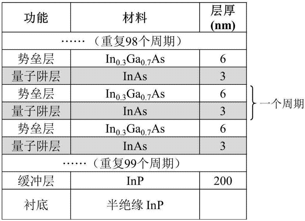
[0038] Growth of InGaAs strain-compensated quantum well superlattice structure with light absorption long-wavelength cut-off wavelength of 2.1 μm:
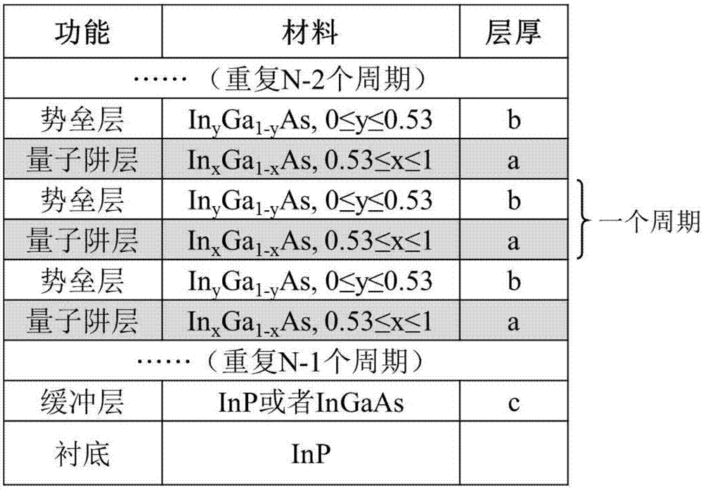
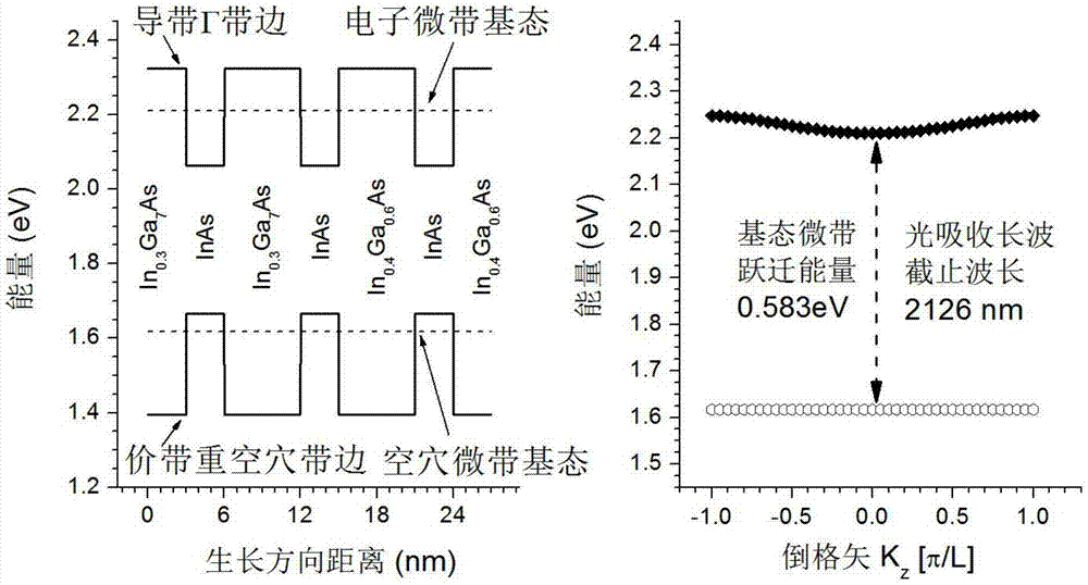
[0039] The purpose of this embodiment is to obtain an InGaAs strain-compensated quantum well superlattice material structure with a light absorption long-wave cut-off wavelength of 2.1 μm. The quantum wells and barrier layers shown in this embodiment are all made of InGaAs single-layer material with a fixed In composition, and neither includes a sub-layer structure. Each superlattice period contains a layer of 3nm thick InAs compressive strain quantum well, a layer of 6nm thick In 0.3 Ga 0.7 As tensile strain barrier. The overall strain compensation of the material is close to 100%. Specific material structures such as figure 2 shown. Its structure contains the following materials in order from bottom to top:
[0040] Material 1: semi-insulating InP (001) substrate.
[0041] Material 2: non-doped InP buffer layer with a th...
Embodiment 2
[0050] Growth of InGaAs strain-compensated quantum well superlattice structure with light absorption long-wave cut-off wavelength of 2.5 μm:
[0051] The purpose of this embodiment is to obtain an InGaAs strain-compensated quantum well superlattice material structure with a light absorption long-wave cut-off wavelength of 2.5 μm. The quantum well shown in this embodiment adopts InGaAs single-layer material with fixed In composition and does not include sub-layer structure. The barrier layer adopts an asymmetric barrier structure, including two InGaAs sublayer structures with different In compositions. Each superlattice period contains three layers of material: the compressive strain quantum well is a layer of InAs with a thickness of 1.53nm, and one side of the quantum well is a layer of InAs with a thickness of 2nm. 0.3 Ga 0.7 As tensile strain barrier, the other side is a layer of 2nm thick In 0.4 Ga 0.6 As tensile strain barrier. The overall strain compensation of the ...
PUM
 Abstract
Description
Claims
Application Information