Check patentability & draft patents in minutes with Patsnap Eureka AI!

Method for imprinting opto-electronic components with bus bars

Active Publication Date: 2017-08-15
HELIATEK GMBH
View PDF19 Cites 0 Cited by
  • Summary
  • Abstract
  • Description
  • Claims
  • Application Information

AI Technical Summary

Benefits of technology

The patent text describes a technical solution for improving the production and use of flexible PV modules by using printed busbars. The invention allows for the creation of flexible PV modules that can be integrated into different objects, such as automobile panes, without needing to be adjusted to their shape. The unconventional design also allows for the creation of transparent components that can be integrated into glass elements. The use of printed busbars overcomes the limitations of conventional methods, resulting in cost savings and high optical absorption coefficients. Overall, the invention provides greater adaptability and flexibility for PV modules, making them more suitable for various applications.

Problems solved by technology

The shadow casting of busbars proves to be disadvantageous, this arising during paste printing on the front side of a photovoltaic module.
Busbars printed from pastes had a defined height and width which cast a shadow on the photovoltaic module upon insolation and thus disadvantageously reduced the efficiency of the module.
The shadow casting is thus minimized, but the solution proves to be unsatisfactory for transparent PV modules.
This method also proves to be unsatisfactory for producing flexible transparent PV modules.

Method used


Image

  • Method for imprinting opto-electronic components with bus bars
  • Method for imprinting opto-electronic components with bus bars
  • Method for imprinting opto-electronic components with bus bars

Examples


Embodiment Construction

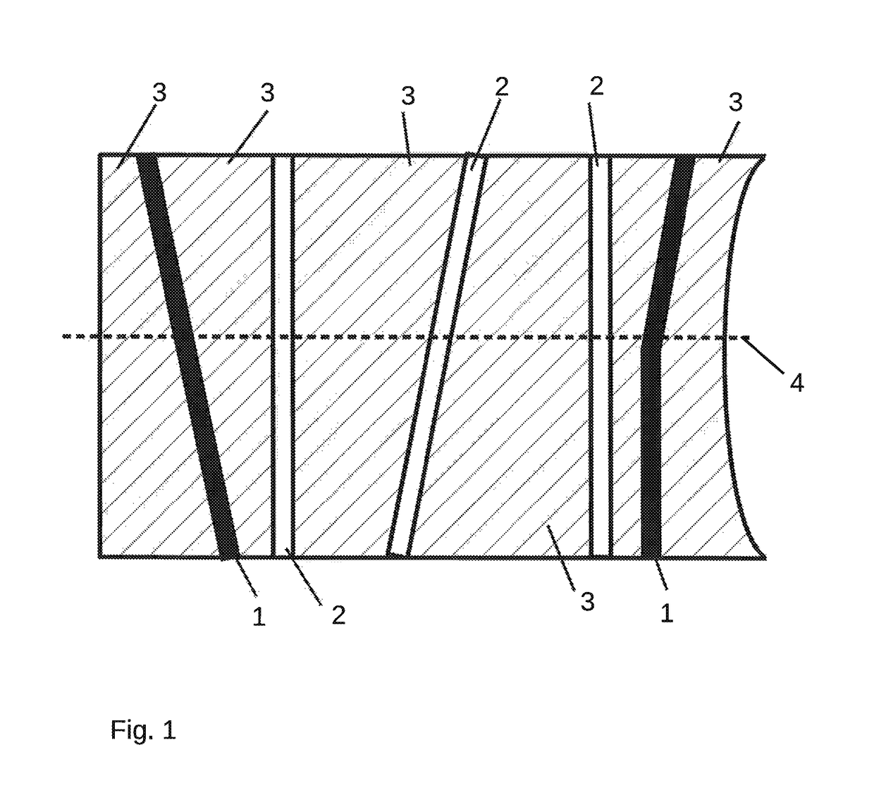
[0026]In one exemplary embodiment, reference is made to the homogeneous color impression and the configuration in free shapes. FIG. 1 illustrates the shapeless configuration of the busbars. Depending on the area of application, they can follow the shape of the PV module. An oblique and angled busbar 1 is visible in the present case. These busbars follow the layout of the conductive layer 3, which was structured by means of laser cutting, scribing or lithographic processes.

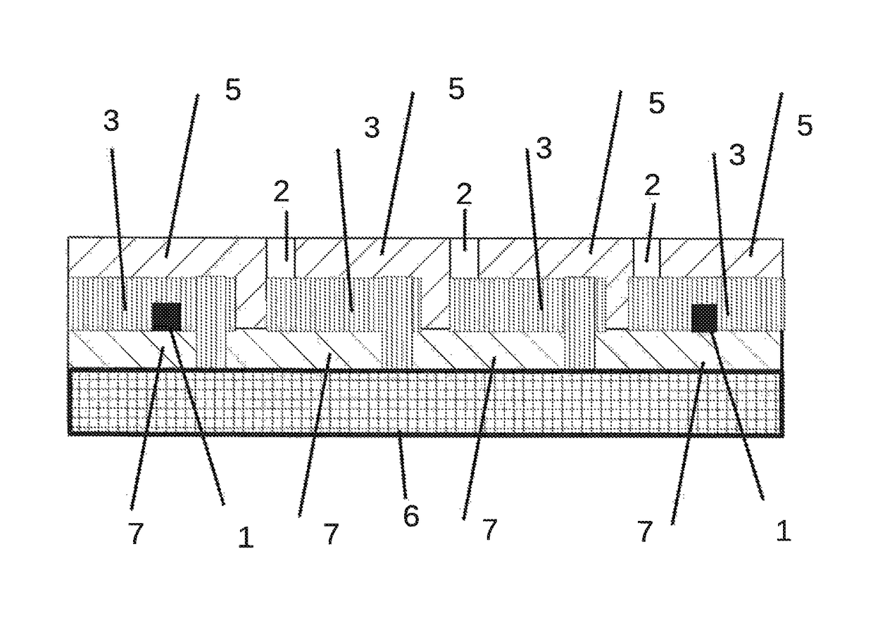
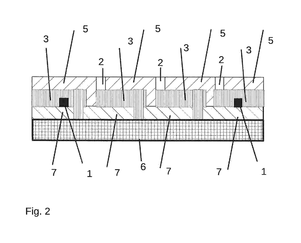
[0027]FIG. 2 illustrates the construction of an organic PV module in cross section 4, wherein a homogeneous color impression is produced on the rear side of the module. A substrate film 6 serves as basic material. The front electrode 7 can be structured before or after the application of the busbars. The busbars 1 are applied to the front electrode 7 by means of printing methods.

[0028]The further process is distinguished by the vapor deposition of the active layer 3, for example a general absorber layer, in vacuo. ...


PUM


Abstract

In a method for imprinting optoelectronic components with at least one bus bar, the bus bar following the shape of the optoelectronic component and allowing a homogeneous color impression on the rear face of the component, the bus bar is printed on a basic material before deposition of a photoactive layer. The basic material may comprise a substrate, or an electrically conductive transparent layer on a substrate. Subsequently, a conductive layer on the substrate is structured to form isolated regions, the photoactive layer is deposited and structured, and then a counter electrode is applied and structured.

Description

CROSS REFERENCE TO RELATED APPLICATIONS[0001]This application is the U.S. National Filing of PCT Application No. PCT / IB2013 / 059257 filed on Oct. 10, 2013 and published in German as WO 2014 / 060912 A1 on Apr. 24, 2014, which claims priority of German patent application number 10 2012 109 777.1 filed on Oct. 15, 2012, the entire disclosure of these applications being hereby incorporated herein by reference.BACKGROUND ART[0002]The invention relates to a method for imprinting optoelectronic components with at least one busbar, wherein the busbar follows the shaping of the optoelectronic component and enables a homogeneous color impression on the rear side of the component.[0003]Optoelectronics is composed of the fields of optics and semiconductor electronics. It encompasses systems and methods which enable the conversion of electronically generated data and energies into light emission or convert light emissions into energy. Optoelectronic elements, in particular organic photovoltaic mod...

Claims


Application Information

Patent Timeline
IPC IPC(8): H01L51/56H01L51/00H01L51/52H01L51/44H01L27/32
CPCH01L51/0022H01L51/445H01L51/5212H01L51/5228H01L51/56H01L27/3204H01L27/3237Y02E10/549Y02P70/521H10K59/86H10K59/10H10K71/611H10K30/83H10K50/814H10K50/824Y02P70/50H10K71/00
Inventor WICHTENDAHL, RALPHBORKERT, ANDREAS
Owner HELIATEK GMBH
Features
  • R&D
  • Intellectual Property
  • Life Sciences
  • Materials
  • Tech Scout
  • Unparalleled Data Quality
  • Higher Quality Content
  • 60% Fewer Hallucinations
Learn More