Method and device for reduced read latency of non-volatile memory

a non-volatile memory and read latency technology, applied in the field of non-volatile memory devices, can solve the problems of inability to perform read and write operations simultaneously, slow application execution, and unsatisfactory real-time application read latency, and achieve the effect of reducing read latency

Active Publication Date: 2009-07-14
MEMORY TECHNOLOGIES LLC
View PDF17 Cites 43 Cited by
  • Summary
  • Abstract
  • Description
  • Claims
  • Application Information

AI Technical Summary

Benefits of technology

[0006]To allow for lower read latency when accessing NAND flash memories, an additional set of commands and / or registers may be defined to be supported by the flash memory device. By means of this command and / or register set, a “virtual” port is created in addition to the existing data ports of the memory controller. This is accomplished by controlling any read / write commands in a memory device such that a read request can be handled while a write / erase operation is in process. The control may be applied with two or more NAND chips, wherein the memory controller handles the read-while write in a way that it is capable of reading from one chip while writing / erasing on another chip; or, alternatively, with NAND chips having additional functionality, such as real read-while-write access or suspend capabilities, where only one such NAND chip is needed and the memory controller may read and write on separate blocks of that one chip or suspend a write operation before performing a read operation.

Problems solved by technology

This causes read latency which might not be desirable or acceptable for real time applications.
In NAND flash memory systems, paging-on-demand is commonly applied, but a major drawback of systems for this technique is that read and write operations cannot be performed simultaneously.
Each page retrieval operation will block the whole system until the page is fully loaded, which slows application execution down considerably.
Any of the described features and problems are present in both memory cards and embedded mass storage devices based on flash memory.

Method used


Image

  • Method and device for reduced read latency of non-volatile memory
  • Method and device for reduced read latency of non-volatile memory
  • Method and device for reduced read latency of non-volatile memory

Examples


Embodiment Construction

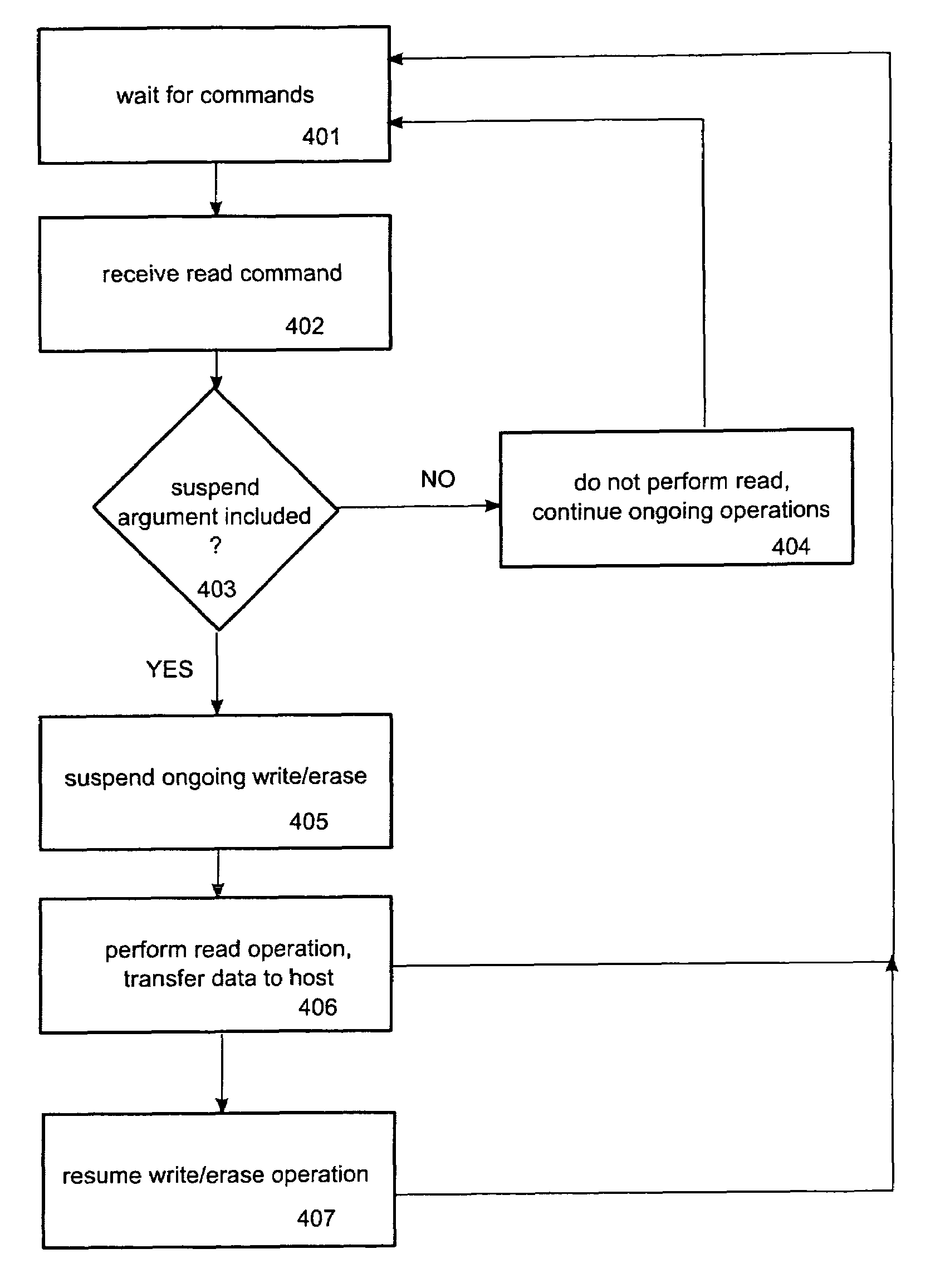
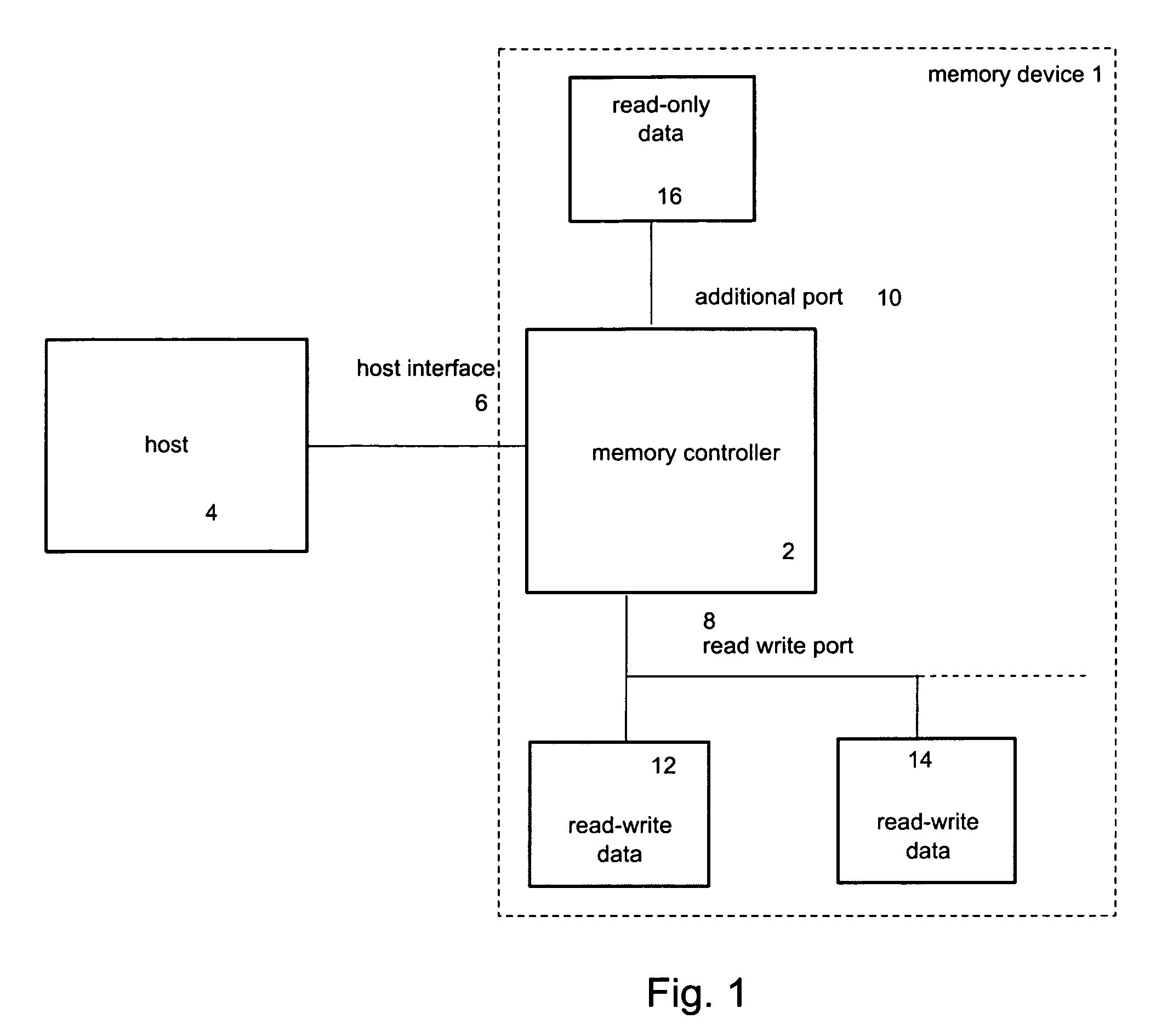
[0012]In FIG. 1, the arrangement according to the invention is shown schematically. The non-volatile memory device 1 comprises at least one NAND type flash memory chip 12, 14, 16 and a memory controller 2 which has a interface to an external host 4. The external host device 4 may be represented by a terminal comprising a processor for executing program code stored in a storage medium. The host may need information stored on the memory device 1 to execute program code or to display the information on the host, such as an internal flash memory or a flash memory card in a mobile communication terminal. The host may be capable of controlling this memory access and to communicate data with the memory device. For this purpose, the host is connected to the memory controller or, alternatively, directly to the memory device if the host is responsible for all access controls and if the structure of the memory device does not require a separate controller. The host may for example be a desktop...


PUM


Abstract

Systems, apparatuses and methods for controlling access operations in a memory device that may include a memory controller(s) and memory. Commands, registers and / or other mechanisms may be defined to be supported by the memory device, where such commands, registers, and / or other mechanisms facilitate the control of read and write / erase operations to allow these operations to be performed simultaneously. Thus, a write and / or erase operation may be initiated on a first memory, a read operation initiated by a set of commands on a second memory, wherein the read and write / erase operations are performed substantially at the same time.

Description

FIELD OF THE INVENTION[0001]This invention relates to non-volatile memory devices, particularly flash memory devices with NAND architecture and more particularly to a method for reducing latencies of NAND flash memory access operations by an additional set of commands and / or registers.BACKGROUND OF THE INVENTION[0002]A flash memory device, such as those used in mobile terminals, usually has multiple partitions. These partitions may be binary partitions (read only) and read-write partitions. During write operations, data cannot be read from the memory until the write operation is completed. This causes read latency which might not be desirable or acceptable for real time applications. In any application, overall system performance will be faster if data can be read from read-only partitions while write operations are in process;[0003]One example of an application where read latency is critical is the paging-on-demand-technique, where pages of data are not copied from a data storage t...

Claims


Application Information

Patent Timeline
Patent Type & Authority Patents(United States)
IPC IPC(8): G06F12/00
CPCG11C7/1075G11C7/22G11C16/26G11C16/10G11C2216/22G11C2216/20G11C16/0483G11C16/14
Inventor GYL, YEVGENHAKKINEN, JUSSIMYLLY, KIMMO
Owner MEMORY TECHNOLOGIES LLC
Why Eureka
Try Eureka