This helps you quickly interpret patents by identifying the three key elements:
Problems solved by technology
Method used
Benefits of technology
Benefits of technology
The present invention provides a method for operating a storage device that can efficiently set read reference voltages to prevent read errors while considering external factors such as thermal stress, keeping time, and word line loading effect. By adjusting default read reference voltages according to various use conditions, read operations can be performed without causing read errors and reducing read latency and power consumption for NAND flash memory.
Problems solved by technology
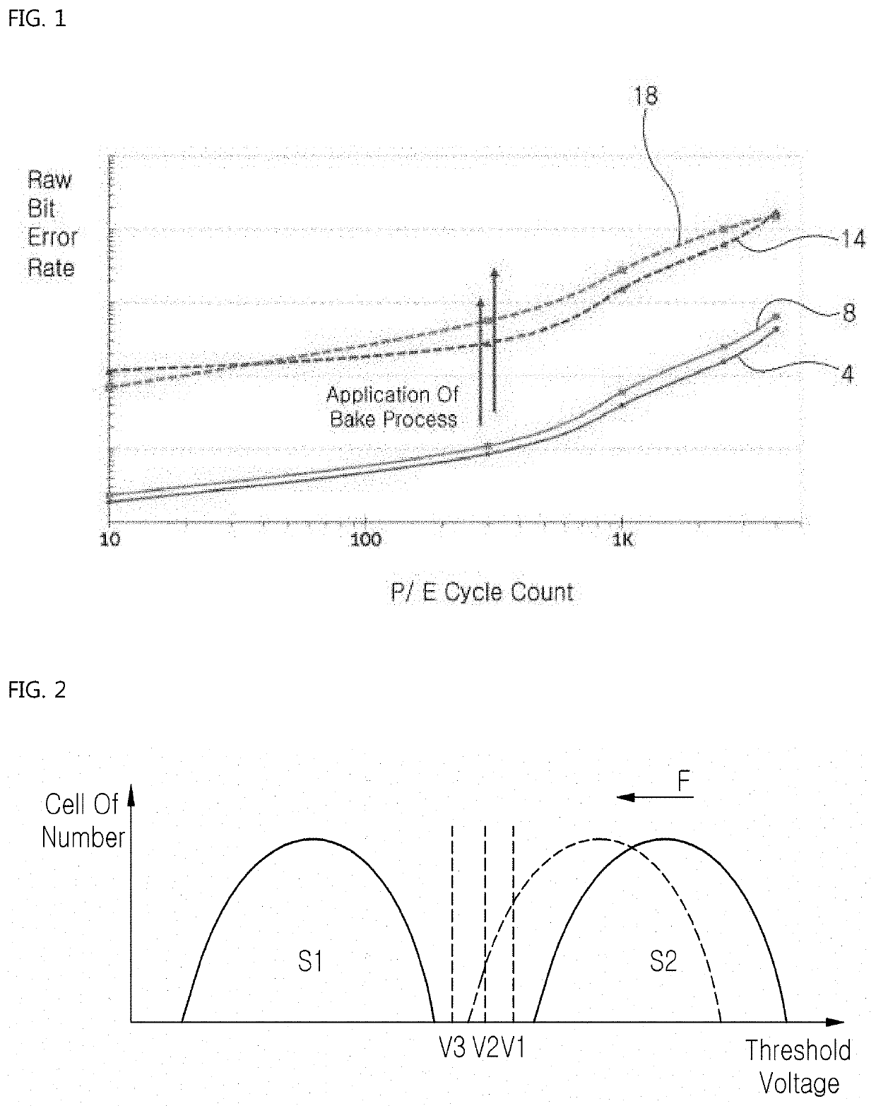
The overall reliability of a NAND flash memory-based storage device gradually degrades with use, due to frequent operations, device aging over time, and external factors such as environmental temperature.
As the number of P / E cycle counts of the NAND flash memory increases, the NAND flash memory cells suffer unintentional parasitic charge traps, or internal rearrangement or migration of stored charge in the cells, resulting in shifting of threshold voltage distributions of the NAND flash memory cells.
Therefore, the charge state of the cell will be misread as a different logical value from the originally written, resulting in a raw bit error.
The cells of a NAND flash memory mounted in the storage device experience the charge loss which is accelerated by a high ambient temperature during manufacturing processes, delivery, or storage thereof.
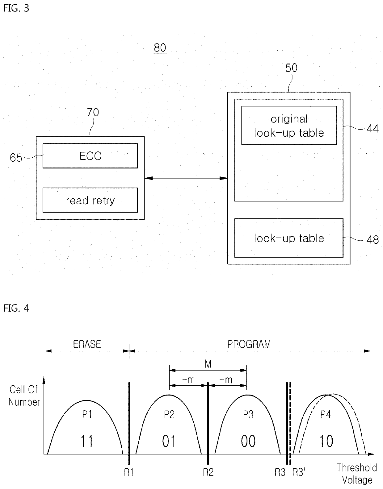
Therefore, the tail portion of the distribution of the threshold voltage state S2 is the cause of increasing the read latency of the NAND flash memory.
However, this process significantly lowers the overall read performance of the NAND flash memory cells.
Method used
Image
Click on the blue label to locate the original text in one second.
Reading with bidirectional positioning of images and text.
Examples
first embodiment
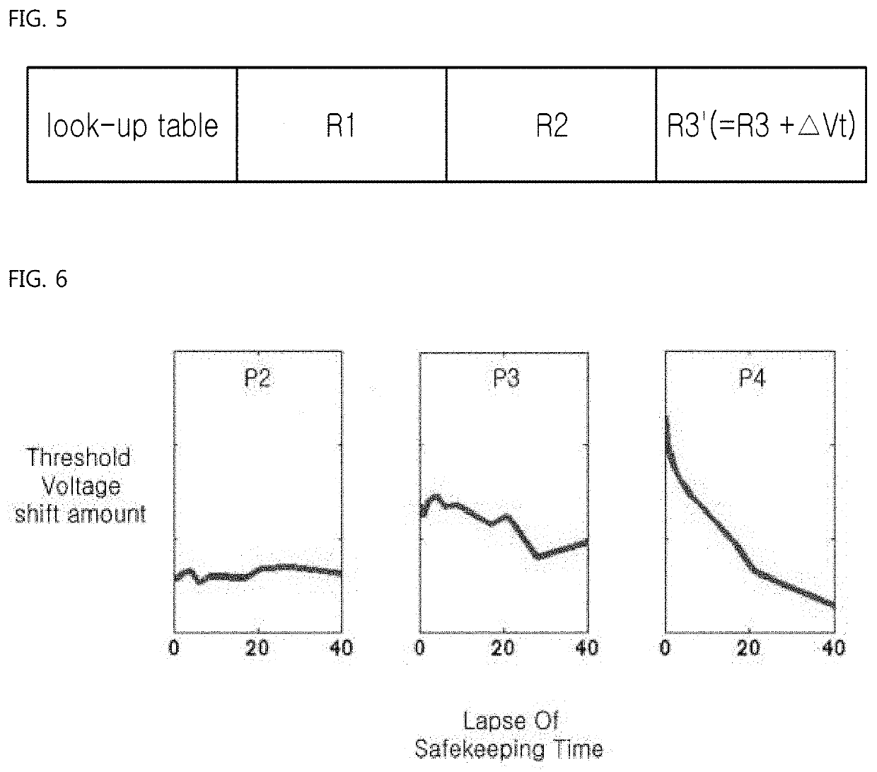
[0044]FIGS. 4 and 5 illustrate a read retry algorithm according to the present invention which is to be embedded in the storage device of FIG. 3.
[0045]Referring to FIGS. 4 and 5, the read retry algorithm adjusts the default read reference voltages R1, R2, and R3. The adjustment of the default read reference voltages R1, R2, and R3 is performed in accordance with actual use conditions of the storage device 80 on the basis of a threshold voltage distribution graph of FIG. 4.
[0046]The adjustment of the default read reference voltages can be performed in accordance with use conditions of the storage device 80, for example, particularly taking into account: pre-treating stress generated to the NAND flash memory 50 during a thermal endurance test performed by the manufacturer of the NAND flash memory 50 after the NAND flash memory 50 is manufactured; heat stress generated to the NAND flash memory 50 while the NAND flash memory 50 is mounted in the storage device 80 using a surface mountin...
second embodiment
[0055]FIGS. 6 to 8 illustrate a read retry algorithm according to the invention, to be used in the storage device of FIG. 3.
[0056]Referring to FIGS. 6 to 8, the read retry algorithm is configured to adjust the default read reference voltages R1, R2, and R3 (refer to FIG. 4). The adjustment of each of the default read reference voltages R1, R2, and R3 is performed by the controller 70 on the basis of a threshold voltage distribution graph (refer to FIG. 4). The adjustment is performed according to a read error margin M between two adjacent threshold voltage states P1 and P2, or P2 and P3, or P3 and P4.
[0057]The adjustment of the default read reference voltage for each threshold voltage stat is performed according to a read error margin M between two adjacent threshold voltage states P1 and P2, P2 and P3, or P3 and P4, and a retention degradation stage of the NAND flash memory 50, which is determined on the basis of the elapsed time after the NAND flash memory 50 is manufactured by th...
third embodiment
[0064]FIGS. 9 to 12 illustrate a read retry algorithm according to the present invention, which is to be used in the storage device of FIG. 3, wherein FIG. 9 is a schematic cross-sectional view, FIG. 10 is a perspective view, FIG. 11 is a graph, and FIG. 12 is a table.
[0065]Referring to FIGS. 9 to 12, the read retry algorithm is configured to adjust the positions (i.e., values) of the default read reference voltages (R1, R2, and R3 of FIG. 4). The adjustment of the default read reference voltages is performed by the controller 70. The adjustment is performed according to the read error margin M between the two adjacent threshold voltage states P1 and P2, or P2 and P3, or P3 and P4, and to the location of each word line group of the NAND flash memory 50.
[0066]The adjustment of the default read reference voltages is performed according to the retention degradation stage of the NAND flash memory 50 mounted in the storage device 80 by taking into account the elapsed time after the NAND ...
PUM
Abstract
Disclosed is a method of operating a storage device including a NAND flash memory including memory cells grouped into blocks, each block being divided into pages. According to the method, a controller in the storage device loads, onto a memory region, a look-up table containing first read reference voltage sets corresponding to respective retention degradation stages of the NAND flash memory and second read reference voltages sets corresponding to respective pages which vary in terms of the threshold voltages. Subsequently, the controller performs a read operation on the memory cells on a per-block basis by using the first read reference voltage set corresponding to a current retention degradation stage, the second read reference voltage set corresponding to a current page, or both, until all of the memory cells in a current block are correctly read.
Description
CROSS REFERENCE TO RELATED APPLICATION[0001]The present application claims priority to Korean Patent Application No. 10-2018-0060468, filed May 28, 2018, the entire contents of which is incorporated herein for all purposes by this reference.BACKGROUND OF THE INVENTION1. Field of the Invention[0002]The present invention relates to a method of operating a storage device, the method being capable of minimizing a bit error rate of a NAND flash memory by modifying default read reference voltages, each of which may be initially set to an intermediate point between two adjacent threshold voltage states, while taking into account external factors (e.g., thermal stress, a storage period, and word line loading effect) having an effect on the operation performance of a NAND flash memory-based storage device.2. Description of the Related Art[0003]Generally, a storage device is used as an auxiliary memory for supplementing the memory capacity of a main memory such as a core memory, a read only m...
Claims
Application Information
Patent Timeline
Application Date:The date an application was filed.
Publication Date:The date a patent or application was officially published.
First Publication Date:The earliest publication date of a patent with the same application number.
Issue Date:Publication date of the patent grant document.
PCT Entry Date:The Entry date of PCT National Phase.
Estimated Expiry Date:The statutory expiry date of a patent right according to the Patent Law, and it is the longest term of protection that the patent right can achieve without the termination of the patent right due to other reasons(Term extension factor has been taken into account ).
Invalid Date:Actual expiry date is based on effective date or publication date of legal transaction data of invalid patent.

