Method for fabricating organic electroluminescent display

a technology of electroluminescent display and organic material, which is applied in the direction of vehicle route interaction devices, nuclear engineering, railway components, etc., can solve the problems of reducing the physical gap between the patterns, affecting the quality of the property of the luminescent material forming the organic luminescent layer may be deteriorated, so as to achieve the effect of improving the pattern quality

Inactive Publication Date: 2009-07-21
SAMSUNG DISPLAY CO LTD
View PDF17 Cites 2 Cited by
  • Summary
  • Abstract
  • Description
  • Claims
  • Application Information

AI Technical Summary

Benefits of technology

[0024]It is an objective of the present invention to provide a method for fabricating an organic electroluminescent display having an improved pattern quality.

Problems solved by technology

However, the vacuum evaporative deposition process has a limitation in reducing the physical gap between the patterns and it is difficult to form a minute pattern to tens of μm level which is required against the possible deformation of the mask.
When the optical etching process is applied, although it is possible to form the minute pattern, the property of the luminescent material forming the organic luminescent layer may be deteriorated by the developing solution or the etching solution.
Therefore, when an inappropriate material is added, the quality of the device may suffer deathblow.
Since the luminescent material used for the organic electroluminescent display has a molecular weight above 10,000 and a Tg value above 100° C., it is relatively difficult to perform the process for forming the organic luminescent layer when compared with the process for forming the color layer.
Therefore, to form such a thin organic luminescent layer, scrupulous care in setting a laser beam transferring condition and an energy distribution is further required.

Method used


Image

  • Method for fabricating organic electroluminescent display
  • Method for fabricating organic electroluminescent display
  • Method for fabricating organic electroluminescent display

Examples


Embodiment Construction

[0055]Preferred embodiments of the present invention will be described in detail with reference to the accompanying drawings.

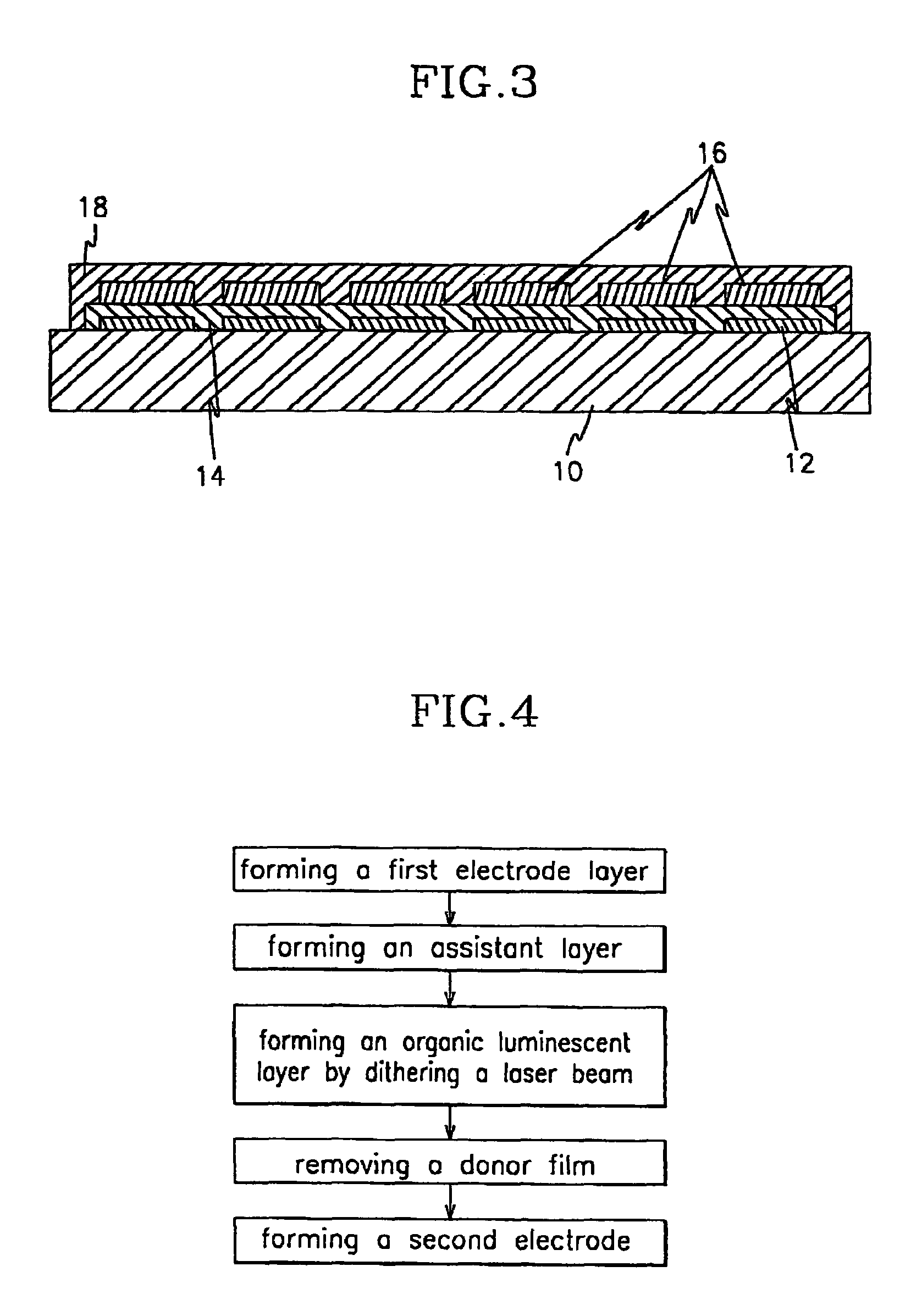
[0056]FIG. 3 shows an organic electroluminescent display fabricated under the present invention, and FIG. 4 shows a method for fabricating an organic electroluminescent display according to a first embodiment of the present invention.

[0057]As shown in the drawings, a first electrode layer 12 having a thickness of about 100-500 nm is formed on a transparent substrate 10 by sputtering ITO (Indium Tin Oxide).

[0058]An assistant layer (hole transport layer) 14 having a thickness of about 10-100 nm is formed on the first electrode layer 12 by, for example, a spin coating process, a dip coating process, a vacuum evaporative deposition process, or a thermal transferring process. An R. G. B organic luminescent layer 16 is formed on the assistant layer (hole transport layer) 14 by a thermal transferring process according to a feature of the present invention. A second e...


PUM

PropertyMeasurementUnit
lateral diameteraaaaaaaaaa

Abstract

In a method for fabricating an organic electroluminescent display, a first electrode layer is formed on a transparent substrate, and a hole transport layer is formed on the first electrode layer. After an organic luminescent layer is formed on the hole transport layer by scanning a donor film disposed on the substrate using a laser beam, the donor film is removed and then a second electrode is formed on the organic luminescent layer. The laser beam dithers while performing the scanning operation to make the energy distribution uniform.

Description

CROSS-REFERENCE TO RELATED APPLICATION[0001]This application is a continuation of U.S. patent application Ser. No. 09 / 935,332, filed Aug. 23, 2001, now U.S. Pat. No. 6,936,300 and claims the benefit of Korean application No. 2000-49287 filed in the Korean Intellectual Property Office on Aug. 24, 2000, the disclosures of which are incorporated herein by reference.BACKGROUND OF THE INVENTION[0002]1. Field of the Invention[0003]The present invention relates to a method for fabricating an organic electroluminescent display that can improve the definition of an image at the edges of a pattern.[0004]2. Description of the Related Art[0005]An electroluminescent display is designed to realize an image by exciting an electroluminescent material disposed between electrodes by applying a voltage to the electrodes. Such an electroluminescent display is classified into an inorganic electroluminescent display and an organic electroluminescent display according to the electroluminescent material. T...

Claims


Application Information

Patent Timeline
Patent Type & Authority Patents(United States)
IPC IPC(8): B05D5/06B05D5/12H05B33/10H01L51/00H01L51/40
CPCH01L51/0009H10K71/162H05B33/10
Inventor LEE, SEONG TAEKKWON, JANG HYUKKANG, TAE MINPARK, JOON YOUNG
Owner SAMSUNG DISPLAY CO LTD
Why Eureka
Try Eureka