Semiconductor device and method for manufacturing the same

a semiconductor device and semiconductor technology, applied in the field of flexible semiconductor devices, can solve the problems of stress generated in the semiconductor device that may damage the element and affect the characteristics of the element, and achieve the effects of reducing the stress exerted on bending with less force, and reducing the damage rate of the element such as the transistor

Inactive Publication Date: 2009-07-28
SEMICON ENERGY LAB CO LTD
View PDF17 Cites 99 Cited by
  • Summary
  • Abstract
  • Description
  • Claims
  • Application Information

AI Technical Summary

Benefits of technology

[0006]In view of the above problem, it is an object of the present invention to provide a semiconductor device which has flexibility and resistance to a physical change such as bending and a method for manufacturing the semiconductor device.
[0014]In the case of forming a semiconductor device having a plurality of integrated circuits which is provided over a flexible substrate, a bending portion is formed between the plurality of integrated circuits or between elements such as transistors included in the integrated circuits. Accordingly, even when external force such as bending is applied to the semiconductor device, the semiconductor device bends with strain selectively generated in the bending portion. Therefore, stress exerted on the element such as a transistor can be reduced, and a damage rate of the element such as a transistor can be decreased. In addition, characteristics of the element such as a transistor can be prevented from being affected. Further, the semiconductor device can be bent with less force by selectively providing a bending portion inside the semiconductor device.

Problems solved by technology

However, when physical force (external force) such as bending is applied from outside to a semiconductor device which is formed by providing an integrated circuit that has an element such as a transistor over a flexible substrate, stress generated in the semiconductor device may damage the element such as a transistor which is included in the semiconductor device and affect characteristics of the element such as a transistor.

Method used


Image

  • Semiconductor device and method for manufacturing the same
  • Semiconductor device and method for manufacturing the same
  • Semiconductor device and method for manufacturing the same

Examples


embodiment mode 1

[0046]In this embodiment mode, one structure example of a semiconductor device of the present invention is explained with reference to drawings.

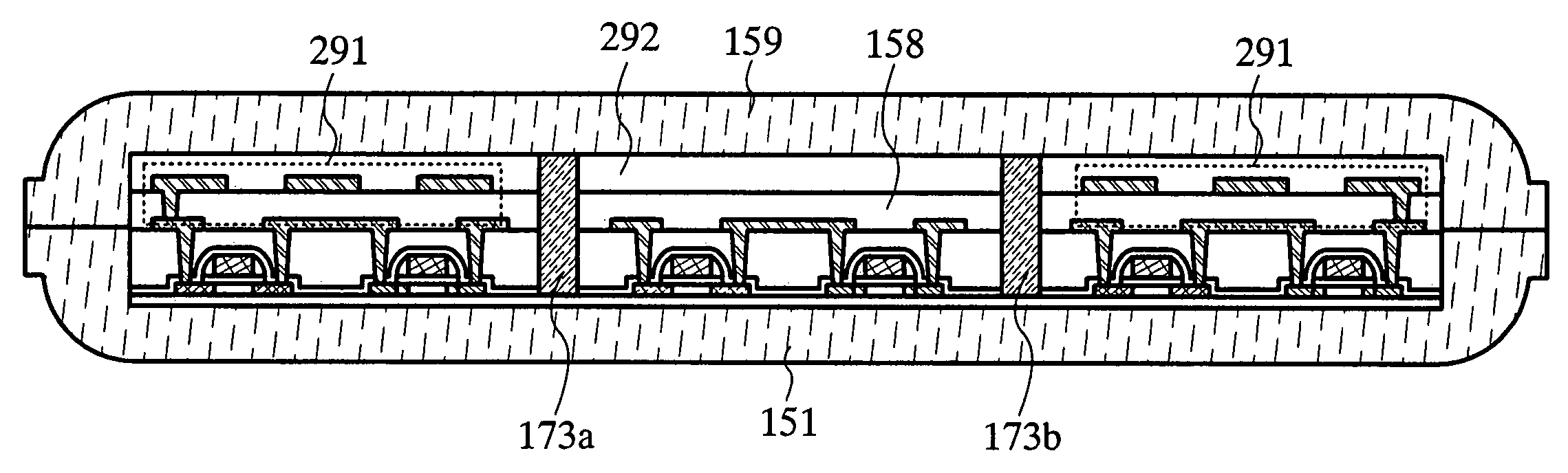
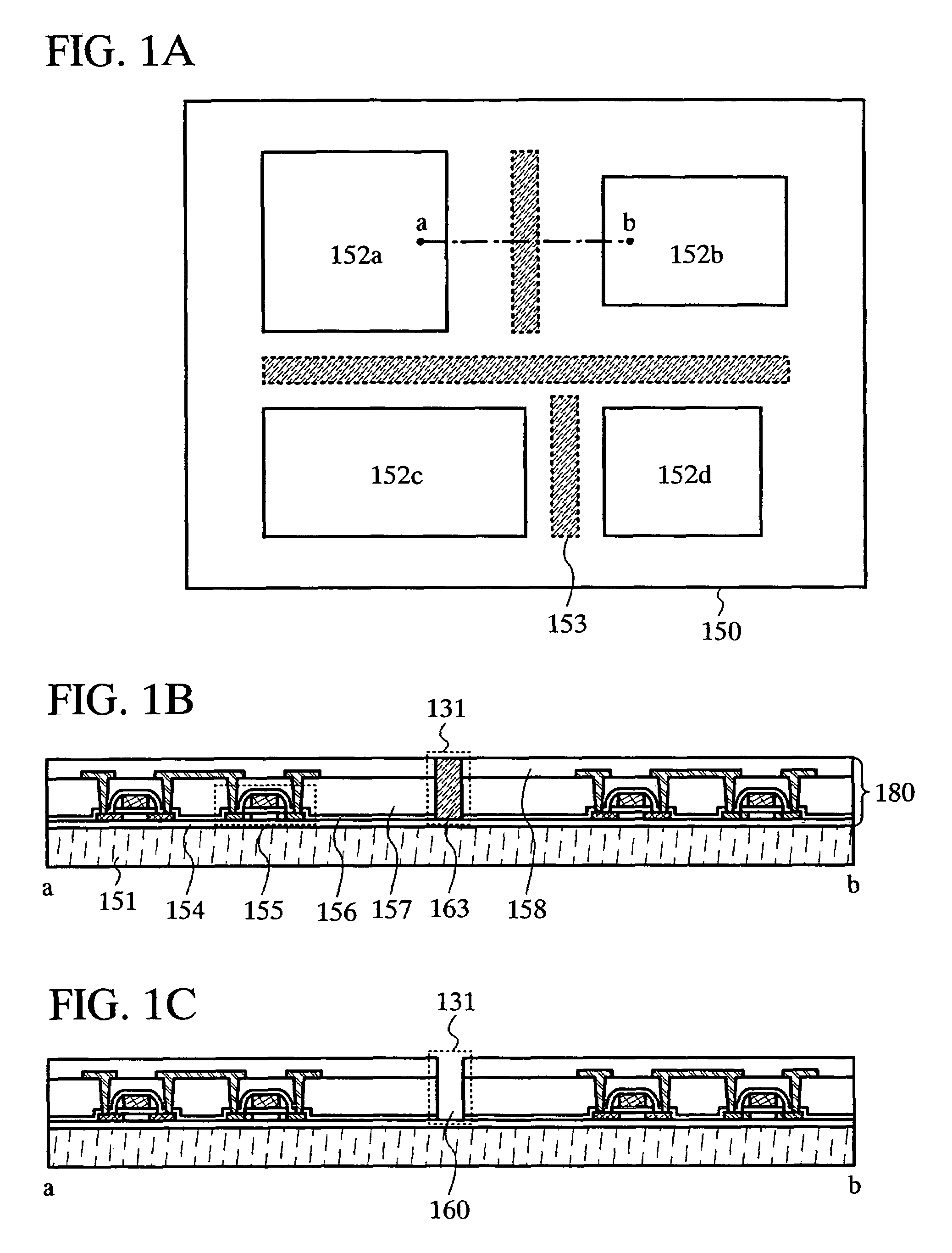
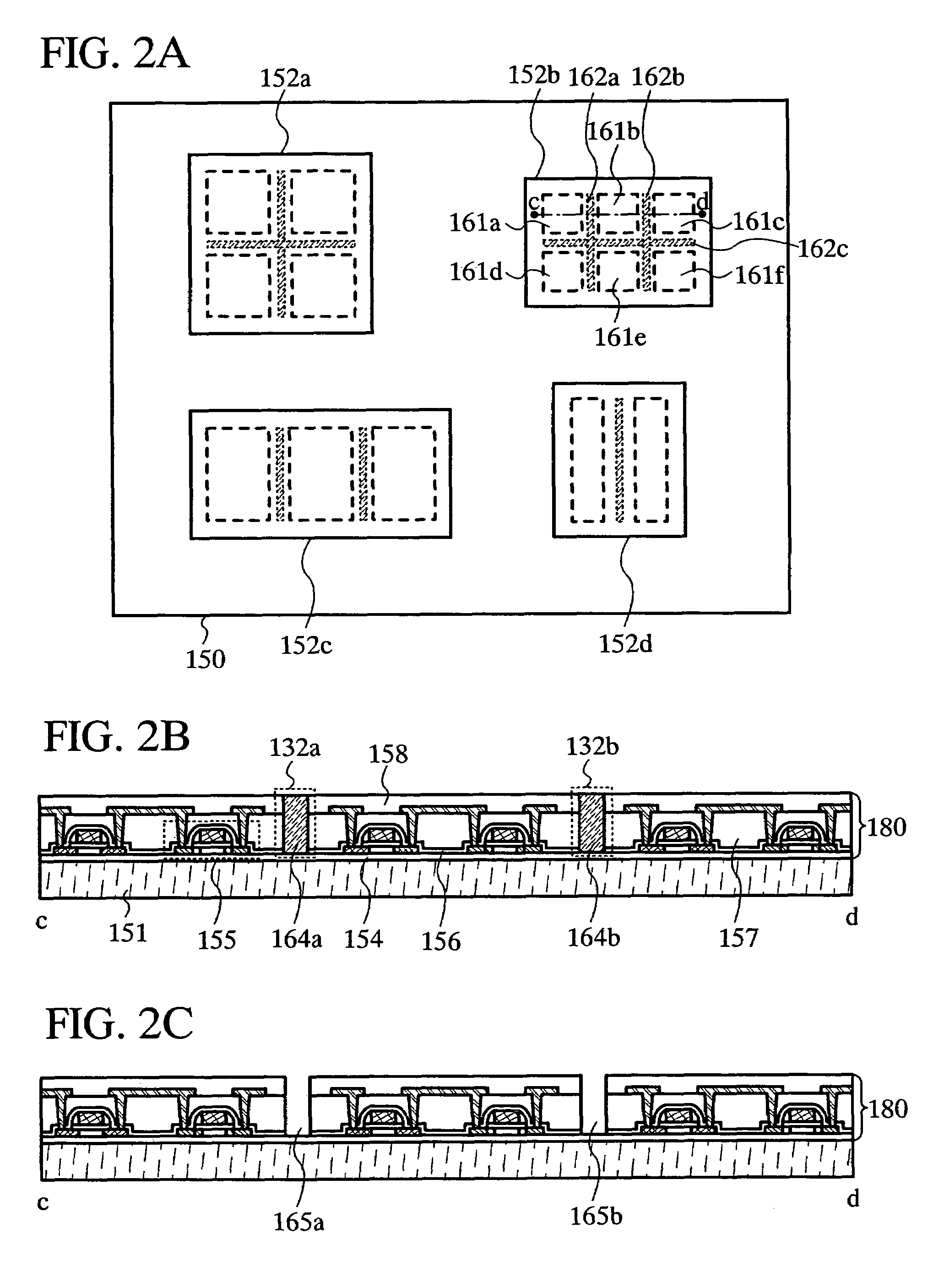
[0047]Generally, a change in shape or volume of an object (also referred to as “strain”) is generated by applying stress to the object. When stress is applied by physical force such as bending to a semiconductor device having an integrated circuit provided over a flexible substrate, the element such as a transistor included in the integrated circuit may be damaged with strain generated, and characteristics of the element such as a transistor may be affected. Therefore, in a semiconductor device 150 which is described in this embodiment mode, a bending portion 153 is provided between integrated circuits 152a to 152d which are provided over a flexible substrate such as a plastic substrate (FIG. 1A). The bending portion 153 may be provided in any manner as long as it is provided between the integrated circuits 152a to 152d. For example, the ben...

embodiment mode 2

[0073]In this embodiment mode, an example of a method for manufacturing a semiconductor device of the present invention is explained with reference to drawings.

[0074]This embodiment mode describes an example of manufacturing a semiconductor device by temporarily providing an element formation layer including an element such as a transistor over a rigid substrate such as a glass substrate, then separating the element formation layer from the rigid substrate using a separation method, and providing the element formation layer over a flexible substrate.

[0075]Here, an example of providing twelve element formation layers 180 over one substrate 170 with a separation layer 171 therebetween and then separating the element formation layers 180 from the substrate 170 is shown (FIG. 3A).

[0076]First, the separation layer 171 is formed over the substrate 170, and the element formation layer 180 including an insulating film 154, a thin film transistor (TFT) 175, an insulating film 156, an insulat...

embodiment mode 3

[0117]In this embodiment mode, a structure of a semiconductor device, which is different from that described in the above embodiment mode is explained with reference to drawings.

[0118]In the case where a transistor is placed alone or nearly alone in an integrated circuit provided in a semiconductor device, damage due to static electricity, damage due to stress from outside, or the like is caused more easily. Thus, by providing a dummy pattern or a dummy transistor formed of a semiconductor of silicon or the like, metal, or the like around the transistor as shown in FIGS. 11A to 11E, destruction of the transistor due to static electricity or stress can be reduced. Hereinafter, an explanation is made with reference to FIGS. 11A to 11E.

[0119]FIG. 11A shows an example of placing dummy transistors 252a and 252b adjacent to a transistor 251 in a source-drain direction thereof. FIG. 11B shows a cross-sectional view taken along line g-h in FIG. 11A. The dummy transistors 252a and 252b can b...


PUM


Abstract

An object of the present invention is to provide a semiconductor device which has flexibility and resistance to a physical change such as bending and a method for manufacturing the semiconductor device. A semiconductor device of the present invention includes a plurality of transistors provided over a flexible substrate, each of which has a semiconductor film, a gate electrode provided over the semiconductor film with a gate insulating film therebetween, and an interlayer insulating film provided to cover the gate electrode, and a bending portion provided between the plurality of transistors, in which the bending portion is provided by filling an opening formed in the interlayer insulating film with a material having a lower elastic modulus, a material having a lower glass transition point, or a material having a higher plasticity than that of the interlayer insulating film.

Description

BACKGROUND OF THE INVENTION[0001]1. Field of the Invention[0002]The present invention relates to a flexible semiconductor device and a method for manufacturing the semiconductor device.[0003]2. Description of the Related Art[0004]Recently, a technique to provide an integrated circuit including a transistor or the like over a flexible substrate such as a plastic substrate has attracted attention. A semiconductor device which is formed by providing an integrated circuit over a flexible substrate can achieve lighter weight, lower cost, or the like as compared to the case of using a substrate such as a semiconductor substrate or a glass substrate. Since a flexible semiconductor device can be bent, the flexible semiconductor device is expected to be applied to various fields and places.[0005]However, when physical force (external force) such as bending is applied from outside to a semiconductor device which is formed by providing an integrated circuit that has an element such as a transi...

Claims


Application Information

Patent Timeline
Patent Type & Authority Patents(United States)
IPC IPC(8): H01L21/46
CPCH01L27/1214H01L27/1266H01L29/78603H01L51/0097H01L27/283Y02E10/549H01L2224/16225H01L2924/12044H01L27/1255H01L27/1218Y02P70/50H10K19/10H10K77/111H01L2924/00
Inventor KOYAMA, JUNDAIRIKI, KOJIOKAZAKI, SUSUMUMORIYA, YOSHITAKAYAMAZAKI, SHUNPEI
Owner SEMICON ENERGY LAB CO LTD
Why Eureka
Try Eureka