Booster circuit

a booster circuit and circuit technology, applied in the field of booster circuits, can solve the problems of deteriorating current supply capability affecting the operation of the pump circuit, and the problem of b>69/b> might encounter a problem, so as to reduce the circuit size of the booster circuit, suppress the amount of boosted voltage, and increase the frequency of the oscillation clock

Inactive Publication Date: 2009-07-28
NORTH PLATE SEMICON LLC
View PDF13 Cites 26 Cited by
  • Summary
  • Abstract
  • Description
  • Claims
  • Application Information

AI Technical Summary

Benefits of technology

[0027]In the above booster circuit, a time period of delay between clocks included in the multiphase clock is generated based on the difference in phase between the oscillation clocks outputted from the oscillation circuit, and therefore always in a proportional relationship with a cycle of the oscillation clocks. Accordingly, even if operating conditions, such as a power supply voltage, variations in process, and temperature fluctuations, are changed, and accordingly, the cycle of the oscillation clocks is changed, the time period of delay is also changed at the same rate. Therefore, a time period of charge transfer for which voltage boosting is performed can be uniquely determined. Thus, it is possible to readily design a booster circuit which allows a desired time period for charge transfer, and also it is possible to increase the frequency of the oscillation clocks.
[0047]As described above, in the booster circuit of the present invention, the time period of delay between clocks and the cycle of the oscillation clocks are always in a proportional relationship with each other, and therefore it is possible to obtain a desired charge transfer time, and increase the frequency of the oscillation clocks. Also, the multiphase clock transfer control circuit can be used to suppress the amount of peak current and thereby to suppress the amount of boosted voltage which overshoots the level of a target voltage. Also, in the case of generating a plurality of boosted voltages, the oscillation circuit and the multiphase clock generation circuit can be shared between the booster blocks, whereby it is possible to reduce the circuit size. Also, the above multiphase clock delay circuit can be used for suppressing the amount of peak current. Also, the boost-assist circuit can be used for reducing the rise time of the boosted voltages. Also, by configuring a first-stage booster cell in a manner as described above, it becomes possible to reduce the circuit size.

Problems solved by technology

However, in the case where the mode suddenly transits from rewrite to read, for example, the pump circuit 69 might encounter a problem as described below when the level of the target voltage is changed.
The above problem is also encountered when the power supply voltage is changed to low level simultaneously as changing the target voltage from high level to low level.
In this case, indeed, the above problem might be readily encountered.
If the above problem is encountered, a desired voltage level cannot be obtained after the level of the target voltage is changed, so that the current supply capability of the booster circuit is deteriorated.
The above-described problem is further readily encountered if the operation voltage of the booster circuit is increasingly reduced.
Accordingly, under given operating conditions, the time period of charge transfer Ttr becomes shorter, resulting in a reduction of voltage boost efficiency.
For the above reasons, it is also difficult to increase the frequency of the oscillation clock 100.

Method used


Image

  • Booster circuit
  • Booster circuit
  • Booster circuit

Examples


Embodiment Construction

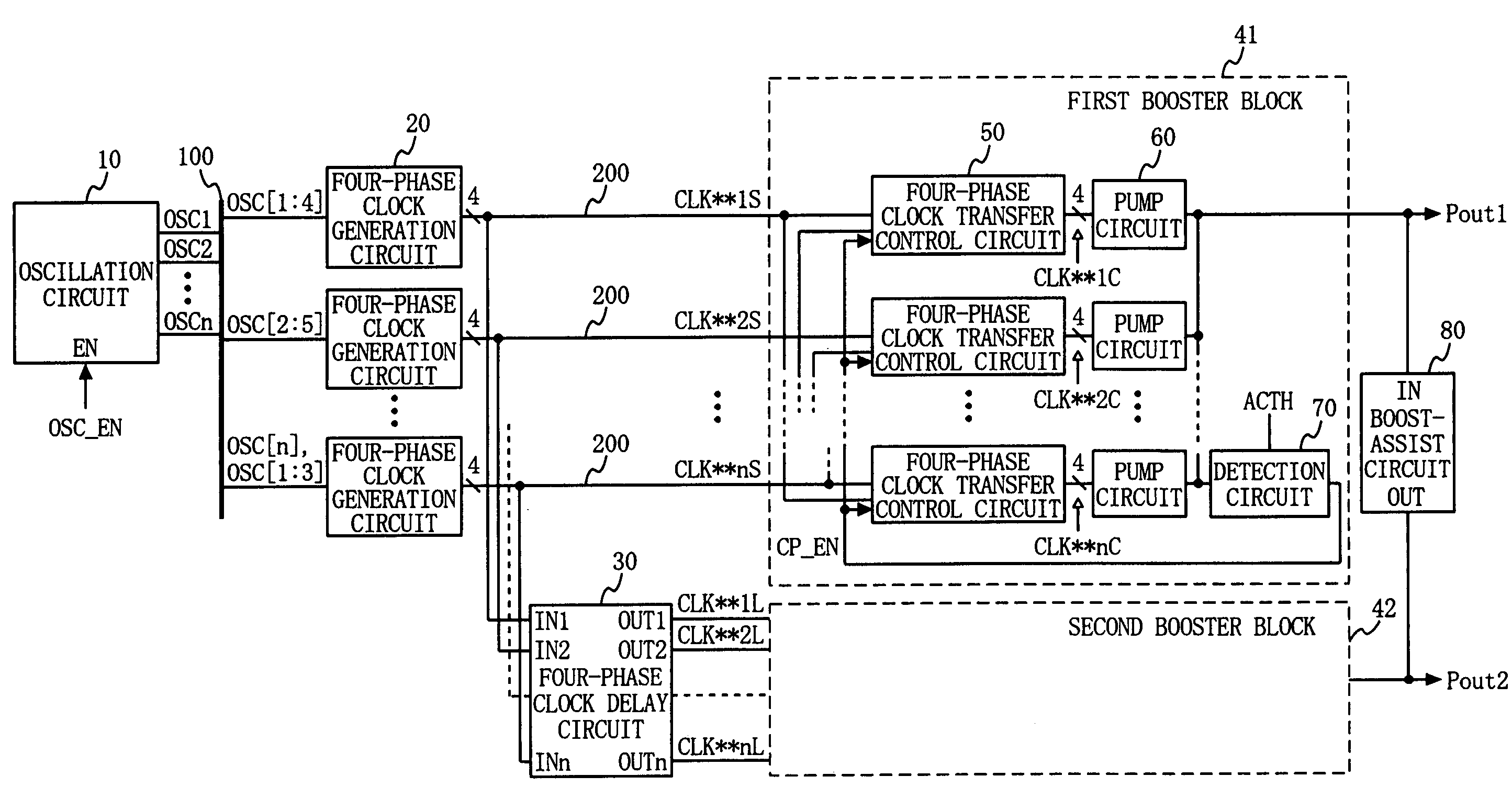
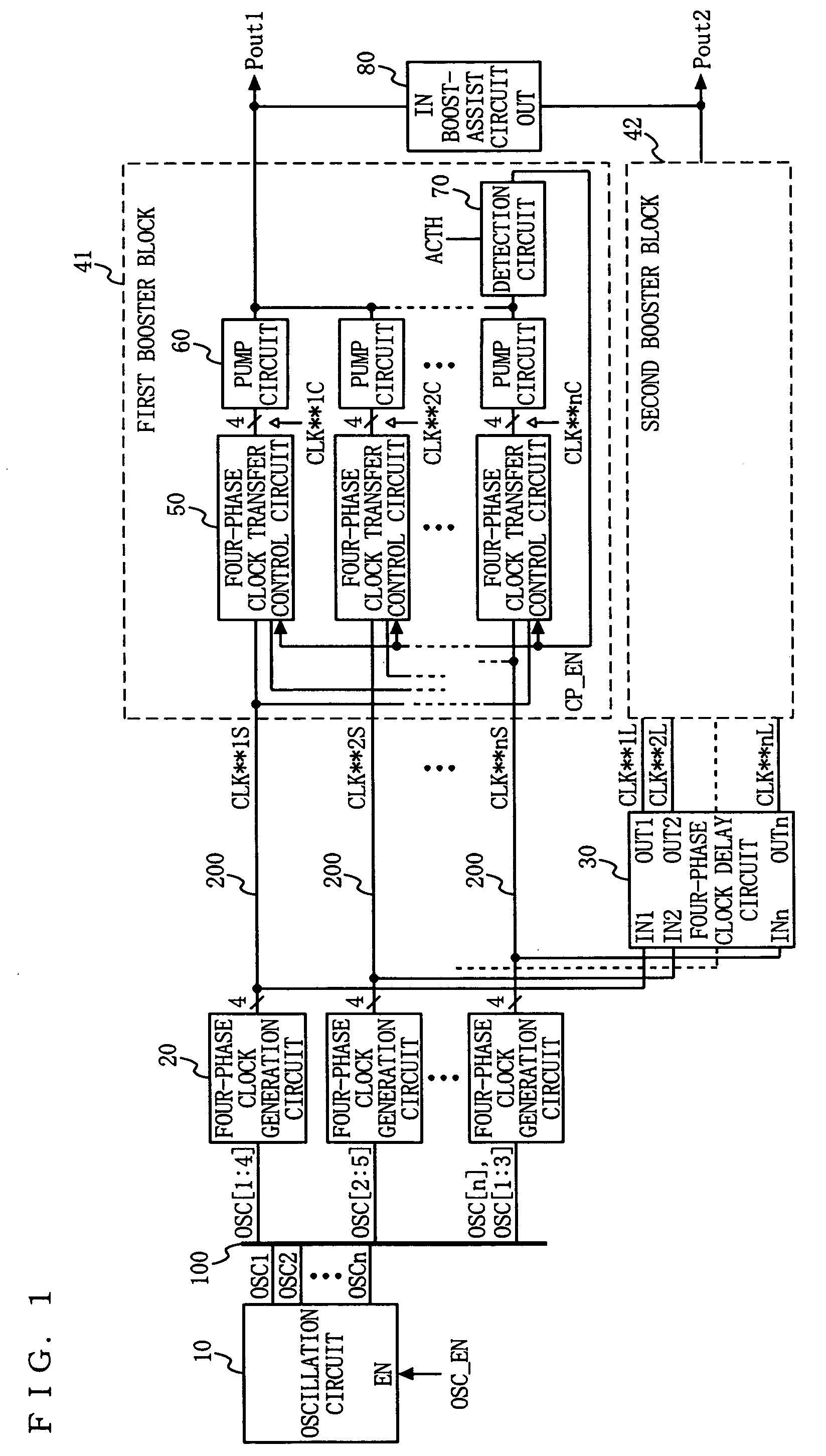
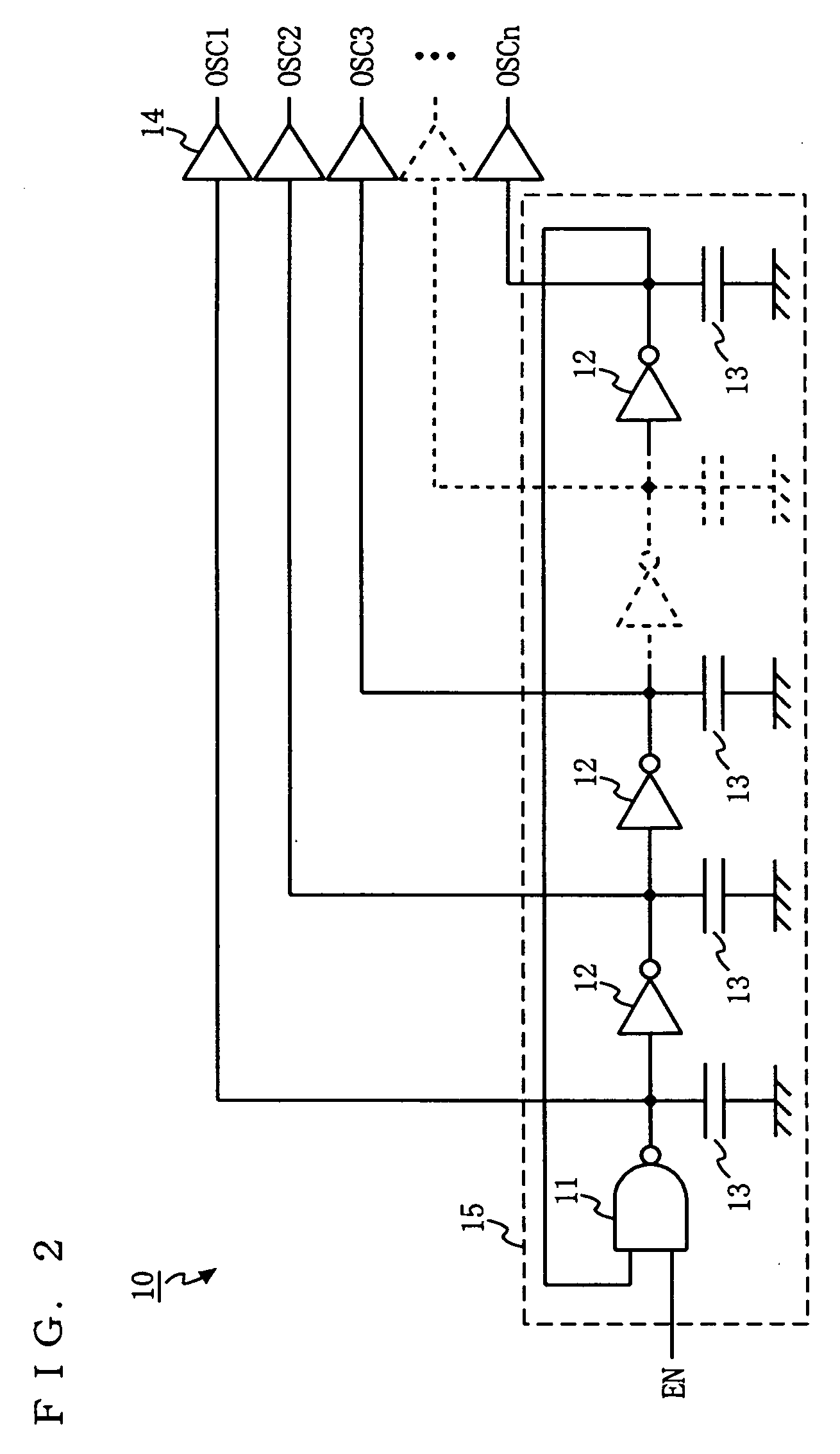
[0068]FIG. 1 is a block diagram illustrating a configuration of a booster circuit according to an embodiment of the present invention. The booster circuit includes an oscillation circuit 10; a plurality of four-phase clock generation circuit 20; a four-phase clock delay circuit 30; a first booster block 41; a second booster block 42; and a boost-assist circuit 80. The first booster block 41 includes four-phase clock transfer control circuits 50 equal in number to the four-phase clock generation circuits 20, pump circuits 60 equal in number to the four-phase clock transfer control circuits 50, and a detection circuit 70. The second booster block 42 is configured in a manner similar to the first booster block 41. The first booster block 41 generates a voltage Pout1 higher than a power supply voltage, and the second booster block 42 generates a voltage Pout2 higher than the voltage Pout1.

[0069]The booster circuit shown in FIG. 1 has the following major features. Specifically, the four-...


PUM


Abstract

An oscillation circuit 10 outputs oscillation clocks 100 different in phase, and a four-phase clock generation circuit 20 generates a four-phase clock 200 based on a difference in phase between the oscillation clocks 100. A four-phase clock transfer control circuit 50 controls whether to transfer the four-phase clock 200 in accordance with a signal CP_EN, and a pump circuit 60 generates a boosted voltage based on the transferred four-phase clock. A time period of delay Tos between clocks included in the four-phase clock 200 is generated based on the difference in phase between the oscillation clocks 100, and therefore always in a proportional relationship with a cycle (Tosc) of the oscillation clocks 100. Accordingly, even if the cycle (Tosc) is changed due to operating conditions, and therefore a time period of charge transfer (Ttr) can be uniquely determined.

Description

BACKGROUND OF THE INVENTION[0001]1. Field of the Invention[0002]The present invention relates to a booster circuit, and more particularly to a booster circuit included in a semiconductor integrated circuit and operating based on a multiphase clock.[0003]2. Description of the Background Art[0004]A nonvolatile memory, such as a flash EEPROM, or a microcomputer including such a memory requires a voltage higher than an externally-supplied power supply voltage in order to perform erase / program operations (hereinafter, collectively referred to as a “rewrite operation”) or a read operation on the nonvolatile memory. The voltage required for such operations is supplied from a booster circuit included in the nonvolatile memory or the like and generating a plurality of boosted voltages. As the booster circuit, a four-phase clock driven threshold balancing-type booster circuit, which is operable at a low voltage level to effectively boost the voltage level, is widely used.[0005]FIG. 16 is a di...

Claims


Application Information

Patent Timeline
Patent Type & Authority Patents(United States)
IPC IPC(8): G05F1/10G05F3/02H01L27/04H01L21/822H02M3/07
CPCH02M3/073H02M2003/077H02M2003/075H02M3/075H02M3/077
Inventor AZUMA, RYOTAROKOJIMA, MAKOTO
Owner NORTH PLATE SEMICON LLC
Why Eureka
Try Eureka