
High resolution monitoring of CD variations

a technology of cd variation and optical metrology system, which is applied in the field of optical methods, can solve the problems of insufficient spatial resolution of average measurement, inability to provide the measurement results requested by memory manufacturers, and difficulty in calculation of thin film and cd parameters from these measurements alone, and achieves high resolution, high accuracy, and larger spot size

Active Publication Date: 2009-07-28
THERMA WAVE INC
View PDF24 Cites 26 Cited by
  • Summary
  • Abstract
  • Description
  • Claims
  • Application Information

AI Technical Summary

Benefits of technology

[0012]In a preferred embodiment discussed in greater detail below, a neural network can be used for correlation. In this method, values from calibration measurements obtained from both technologies are used to train and validate a neural network. Values obtained from the test wafers are then input into the network to produce parameter values. The neural network approach is advantageous since it is very fast and adaptive.

Problems solved by technology

None of these systems, if used alone, currently can provide the measurement results requested by the memory manufacturers.
This average measurement does not have enough spatial resolution to satisfy the demands of the manufacturers.
However, the BPR and BPE systems produce a much smaller set of measurement data making the calculation of thin film and CD parameters quite difficult from these measurements alone.
In addition, given the large number of requested measurement points, performing complex regressions for each of the measurement points would take a quite a long time, longer than would be acceptable to the manufacturers.

Method used


Image

  • High resolution monitoring of CD variations
  • High resolution monitoring of CD variations
  • High resolution monitoring of CD variations

Examples


Embodiment Construction

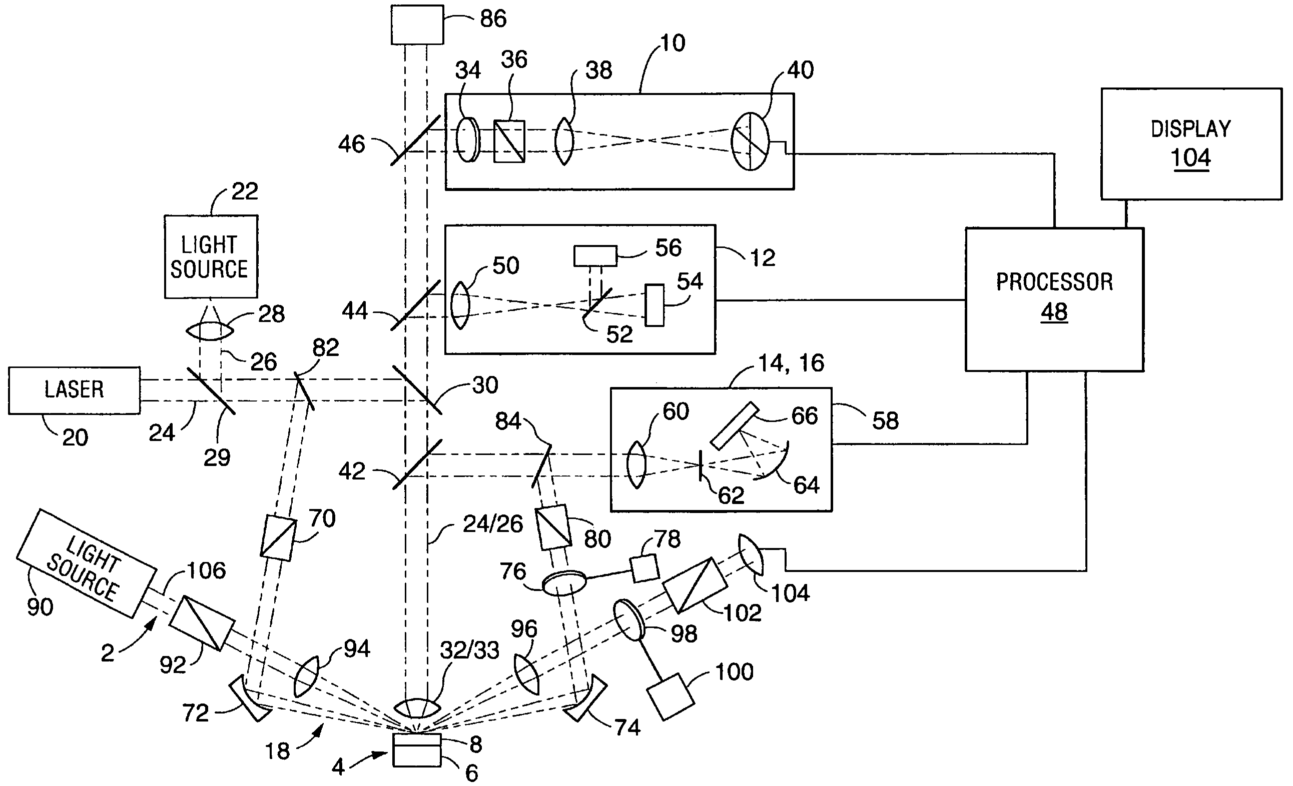
[0034]The metrology industry currently markets tools having more than one type of measurement module on a single platform. The assignees herein market such a device under the name Opti-Probe. This tool is advantageous in that it includes both broadband and laser based metrology technologies. The subject invention can be implemented on this type of tool. The discussion of this particular tool is for illustrative purposes only and should not be limiting. For example, the multiple measurements associated with the subject method could be performed with separate tools rather than a combination tool. Of course, the calibration measurement could be performed with one tool and the test phase measurements performed with a different tool. Using a composite tool for all the measurements can improve accuracy.

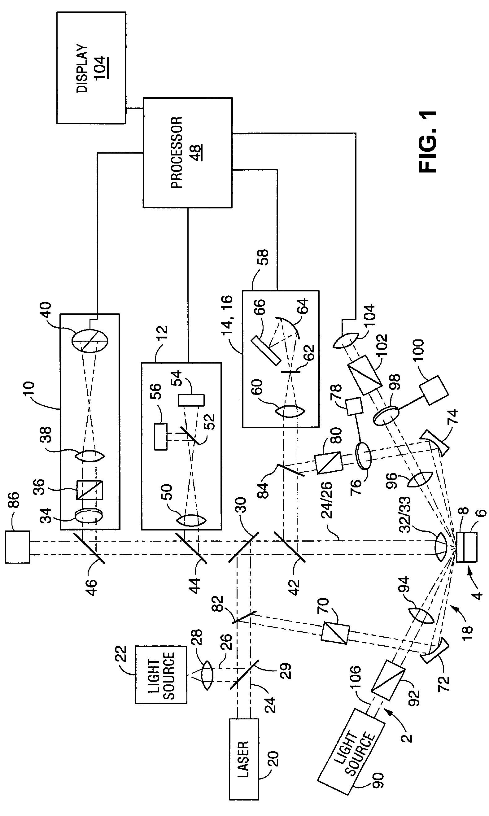
[0035]The basic configuration of this tool is illustrated in FIG. 1. More complete details about this tool can be found in U.S. Pat. No. 6,278,519 incorporated herein by reference. The elem...


PUM

PropertyMeasurementUnit
diameteraaaaaaaaaa
sizeaaaaaaaaaa
angleaaaaaaaaaa

Abstract

An optical metrology method is disclosed for evaluating the uniformity of characteristics within a semiconductor region having repeating features such a memory die. The method includes obtaining measurements with a probe laser beam having a spot size on the order of micron. These measurements are compared to calibration information obtained from calibration measurements. The calibration information is derived by measuring calibration samples with the probe laser beam and at least one other technology having added information content. In the preferred embodiment, the other technology includes at least one of spectroscopic reflectometry or spectroscopic ellipsometry.

Description

PRIORITY[0001]This application claims priority to prior provisional applications Ser. No. 60 / 764,701, filed Feb. 2, 2006, and Ser. No. 60 / 850,603, filed Oct. 10, 2006, both of which are incorporated by reference.TECHNICAL FIELD[0002]The subject invention relates generally to optical methods for inspecting and analyzing semiconductor wafers and other samples. In particular, the subject invention relates to optical metrology system for thin films and critical dimension (CD) measurements.BACKGROUND[0003]Semiconductor memory chips are formed as a plurality of dies on a wafer. Within each die, there are typically a large number of repeating structures (e.g. lines). In contrast, microprocessors formed on semiconductor wafers generally do not exhibit this type of repeating structures (except, for example, in certain regions allocated to microprocessor memory).[0004]As device sizes continue to shrink, memory manufacturers are continuing to seek methods for measuring the uniformity of the re...

Claims


Application Information

Patent Timeline
Patent Type & Authority Patents(United States)
IPC IPC(8): G01B11/14G01N21/00
CPCG01B11/0641G01M11/025G01N21/41G01V8/22G01N21/8806G01N21/9501
Inventor OPSAL, JONGRODNENSKY, ILYAPOIS, HEATH
Owner THERMA WAVE INC
Learn More