Optical filter
a filter and optical technology, applied in the field of optical filters, can solve the problems of filter warping or distortion, warping and distortion becoming more pronounced, and it is difficult to obtain a crystal plate of this thickness, so as to suppress warping or distortion, parallelism and flatness of the principal faces of the optical filter can be markedly improved, and achieve the effect of no
- Summary
- Abstract
- Description
- Claims
- Application Information
AI Technical Summary
Benefits of technology
Problems solved by technology
Method used
Image
Examples
first embodiment
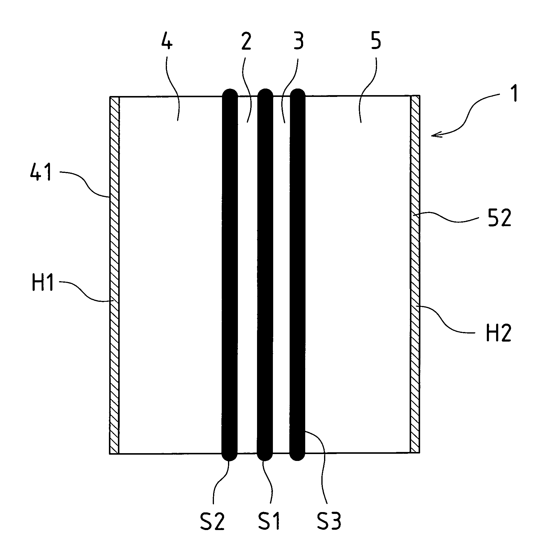
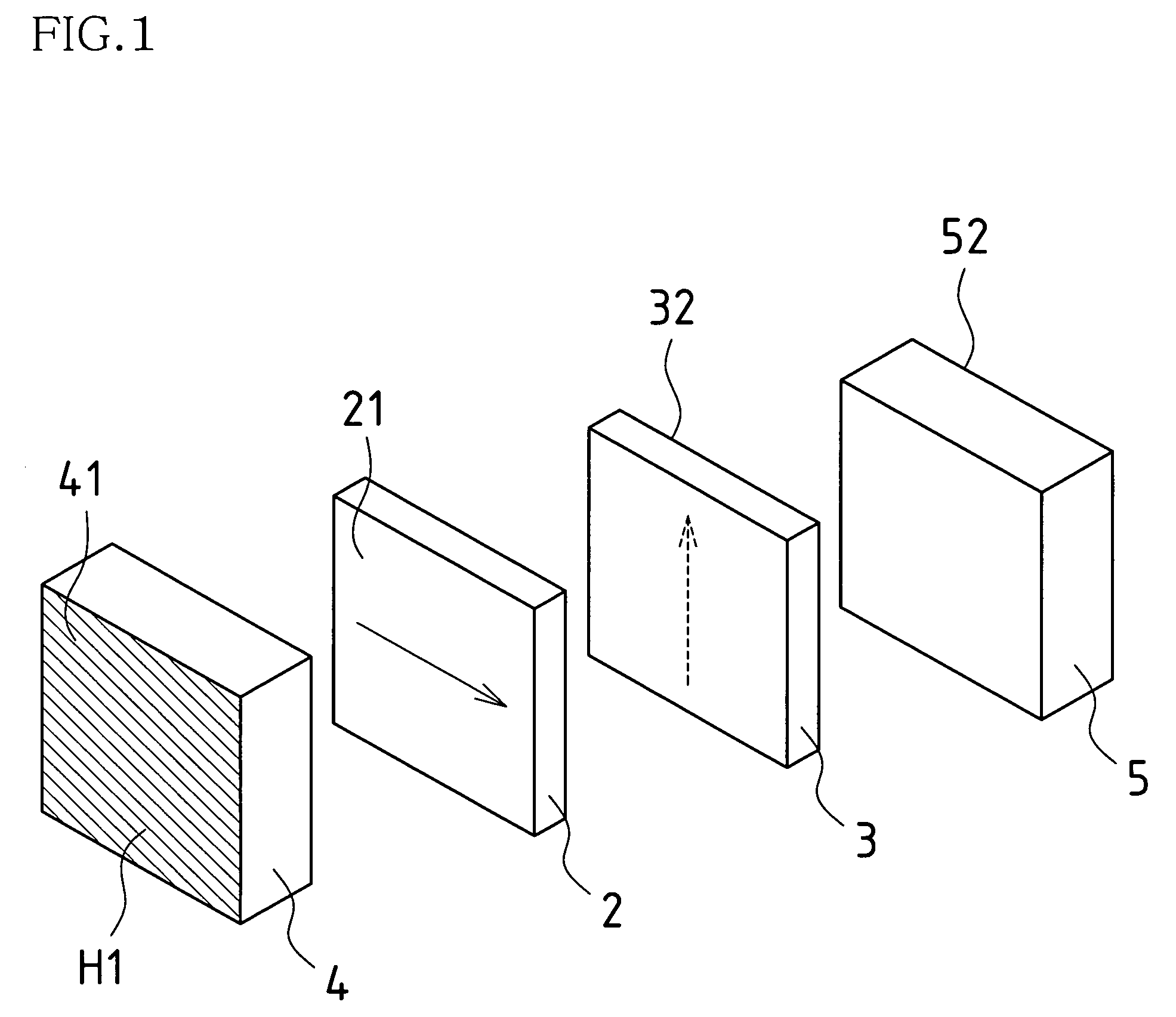
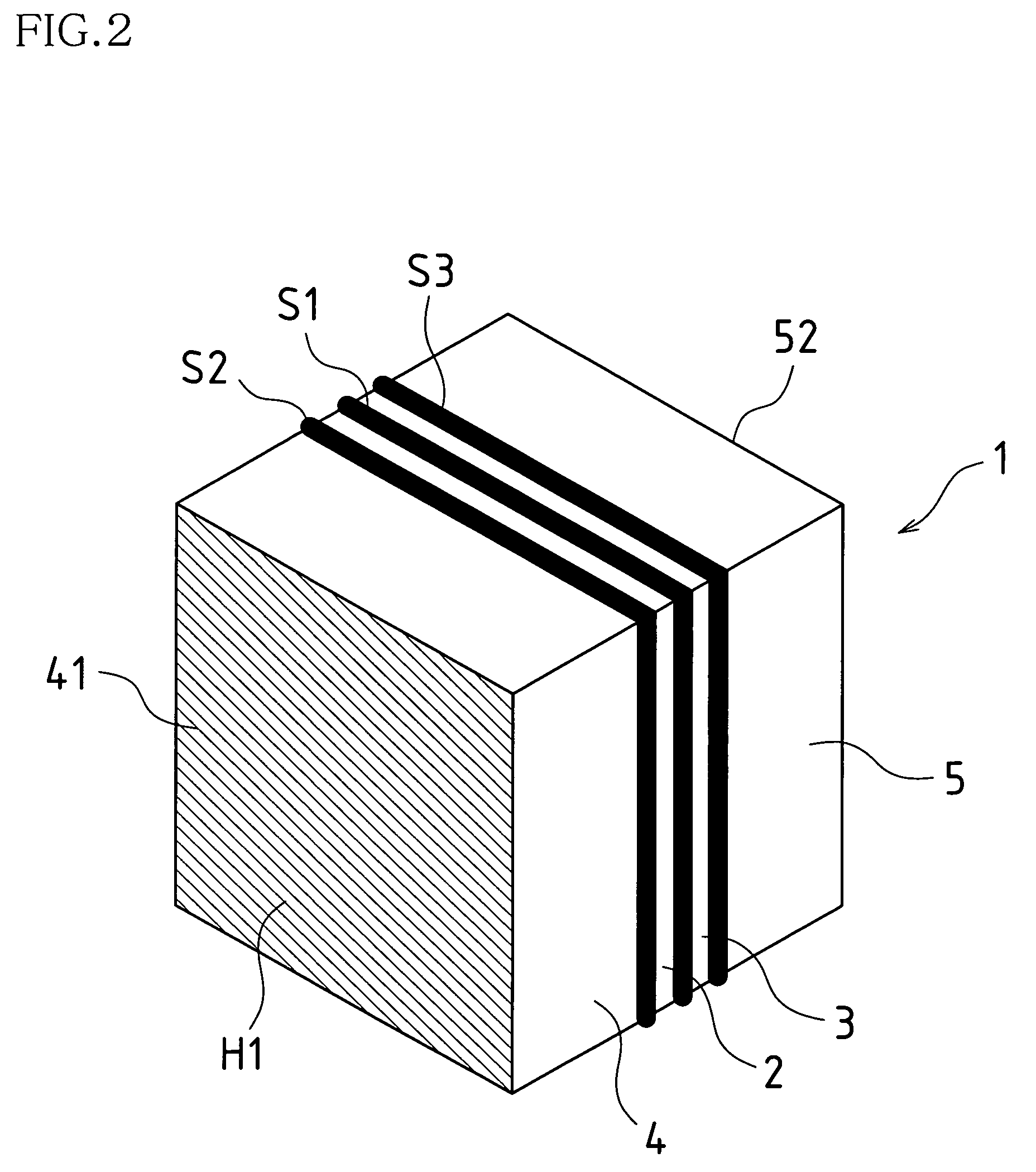
[0049]A first embodiment of the present invention will now be described, using a phase plate as an example, through reference to the drawings. FIG. 1 is an exploded perspective view of the phase plate according to this embodiment, FIG. 2 is a perspective view of the assembled state in FIG. 1, and FIG. 3 is a side view of FIG. 2.
[0050]As shown in these drawings, an optical filter 1 is constituted by two crystal plates (optically anisotropic crystal plates) 2 and 3, and glass substrates 4 and 5. This will now be described in more specific terms. Here, the front side in FIGS. 1 and 2 (the left side in FIG. 3) shall be the incident face (referred to as the incident side end face in the present invention), the crystal plate that is in the front is called a first crystal plate 2, the glass substrate that is in the front is called a first glass substrate 4, the back side (the right side in FIG. 3) shall be the exit face (referred to as the exit side end face in the present invention), the ...
second embodiment
[0056]A second embodiment of the present invention will now be described, using an optical low pass filter as an example, through reference to the drawings. FIG. 4 is an exploded perspective view of the optical low pass filter according to this embodiment, FIG. 5 is a perspective view of the assembled state in FIG. 4, and FIG. 6 is a side view of FIG. 5.
[0057]As shown in these drawings, an optical low pass filter 6 is constituted by a crystal plate (optically anisotropic crystal plate) 7 and glass substrates 8 and 9. This will now be described in more specific terms. Here, the front side in FIGS. 4 and 5 (the left side in FIG. 6) shall be the incident face (referred to as the incident side end face in the present invention), the glass substrate that is in the front is called a first glass substrate, the back side (the right side in FIG. 6) shall be the exit face (referred to as the exit side end face in the present invention), and the glass substrate that is in the back is called a ...
working example 1
[0064]As shown in FIG. 7, the optical filter 6 according to this Working Example 1 includes the crystal plate A, the substrate C, the crystal plate B, the crystal plate D, and the substrate E stuck together, in that order from the left in the drawing, with a UV adhesive S6. The crystal plate A, the substrate C, the crystal plate B, the crystal plate D, and the substrate E here are disposed in an overlapping state. An antireflective film (optical coating) is formed on the exit side end face A1 of the crystal plate A, which corresponds to one side face of the optical filter 6. An infrared-cut coating (optical coating) is formed on the incident side end face E1 of the substrate E, which corresponds to the other side face of the optical filter 6.
[0065]With the optical filter 6 according to this Working Example 1, starting from the left side in FIG. 6, the thickness of the crystal plate A is set to 260 μm, the thickness of the substrate C is set to 1200 μm, the thickness of the crystal p...
PUM
 Abstract
Description
Claims
Application Information


