Optical device with integrated semi-conductor laser source and integrated optical isolator

a semiconductor laser source and optical isolator technology, applied in the direction of instruments, active medium materials, laser details, etc., can solve the problems of unstable laser source, propagation of optical mode, device unsuitability for optical devices,

Active Publication Date: 2009-07-28
WSOU INVESTMENTS LLC
View PDF2 Cites 7 Cited by
  • Summary
  • Abstract
  • Description
  • Claims
  • Application Information

AI Technical Summary

Problems solved by technology

It is known that a laser source can be rendered unstable by a stray optical beam emanating from the initial emission beam and reflected by an optical surface external to the cavity of the laser.
These devices are rather unsuitable for optical devices comprising semi-conductor lasers insofar as they require a certain number of components that are difficult to integrate into devices whose dimensions are of the order of a millimeter.
However, this type of configuration exhibits several major drawbacks.
The electrical contact layer being very near to the active zone, it disturbs the propagation of the optical mode and causes significant optical losses.
The structure of the electrical contacts not being optimized, significant electrical losses can occur, causing local heating.
Finally, the small thickness of the substrate 3 necessary for the operation of the isolator poses technological production problems that are tricky to control.
Moreover, this type of structure has lower performance.

Method used


Image

  • Optical device with integrated semi-conductor laser source and integrated optical isolator
  • Optical device with integrated semi-conductor laser source and integrated optical isolator
  • Optical device with integrated semi-conductor laser source and integrated optical isolator

Examples


Embodiment Construction

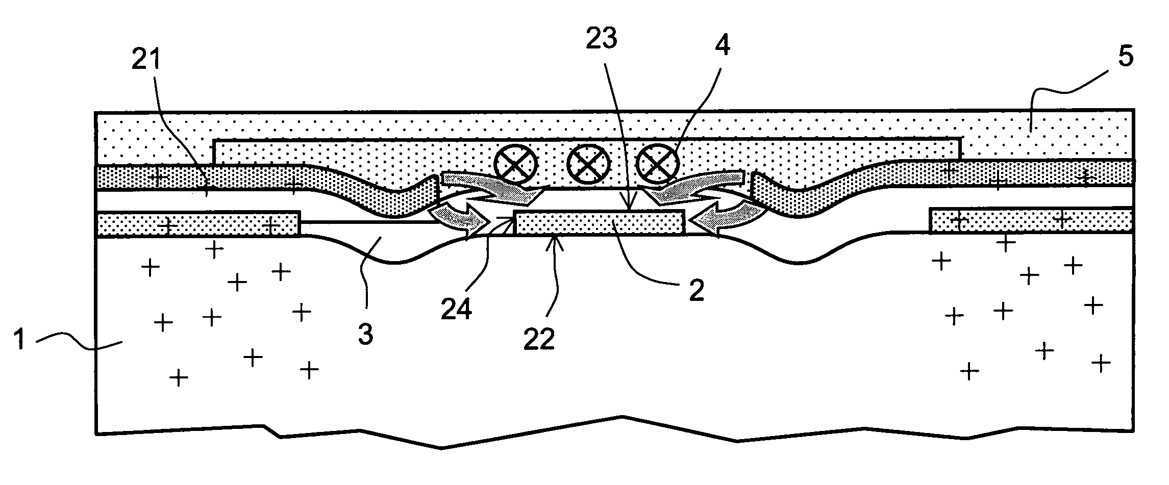
[0054]As has been seen, one of the major drawbacks of structures with optical isolator according to the prior art is that the electrical contact layer is very near to the active zone so that the magneto-optical material is closest to the said zone. This configuration is generally adopted because it makes it possible to easily inject the current into the active zone as indicated by the vertical solid arrows of FIG. 4 representing the current injection.

[0055]The core of the invention is to decouple the current injection means making it possible to ensure the amplification of the SOA, from the magneto-optical means making it possible to ensure the non-reciprocal effect of the isolator. To this end, the electrical contact layer is disposed so that the injection of the charge carriers takes place via the lateral faces and the edges of the upper face of the active layer. Amplification and isolation are thus ensured at one and the same time without having the drawbacks of the devices accor...


PUM


Abstract

The field of the invention is that of optical devices comprising an integrated semi-conductor laser and an integrated optical isolator. These devices are used mainly in the field of digital telecommunications. More particularly, the invention applies to so-called absorption isolators whose complex index is non-reciprocal and depends on the direction of propagation of the light. Generally, integrated optical isolators of this type fulfill two functions. On the one hand, they comprise a magneto-optical layer ensuring the non-reciprocal effect and on the other hand an active zone ensuring the amplification of the laser beam, the injection of the charge carriers into the active zone being ensured by an electrical contact layer. The invention proposes, so as to limit the disturbing effects of the contact layer on the propagation of the laser beam, that the contact layer be eliminated above the active zone and that the injection of the charge carriers be ensured via the lateral faces and the edges of the upper face of the active zone.

Description

BACKGROUND OF THE INVENTION[0001]1. Field of the Invention[0002]The field of the invention is that of optical devices comprising an integrated semi-conductor laser emission source and an integrated optical isolator. These devices are used mainly in the field of high-speed digital telecommunications.[0003]2. Description of the Prior Art[0004]It is known that a laser source can be rendered unstable by a stray optical beam emanating from the initial emission beam and reflected by an optical surface external to the cavity of the laser. Subsequently in the text, a light emission source comprising an optical amplifier of laser type will either be called a laser source or laser. To decrease this phenomenon, an optical isolator is disposed at the exit of the laser. Its function is to allow through the light emanating from the laser and to eliminate any stray light coming in the opposite direction.[0005]Basically, an optical isolator implements a non-reciprocal optical effect making it possi...

Claims


Application Information

Patent Timeline
Patent Type & Authority Patents(United States)
IPC IPC(8): H01S5/00
CPCG02F1/0955H01S5/026H01S5/0064
Inventor ACCARD, ALAINDAGENS, BEATRICE
Owner WSOU INVESTMENTS LLC
Why Eureka
Try Eureka