Phase lock loop device
a phase lock and loop technology, applied in the direction of digital transmission, pulse automatic control, transmission, etc., can solve the problems of unavoidable gain mismatching of internal circuitry, and the pll device b>100/b> cannot ideally lock the clock signal ck, so as to achieve the effect of alleviating degradation and overcoming gain mismatching problem
- Summary
- Abstract
- Description
- Claims
- Application Information
AI Technical Summary
Benefits of technology
Problems solved by technology
Method used
Image


Examples
Embodiment Construction
[0029]The following description is of the best-contemplated mode of carrying out the invention. This description is made for the purpose of illustrating the general principles of the invention and should not be taken in a limiting sense. The scope of the invention is best determined by reference to the appended claims.
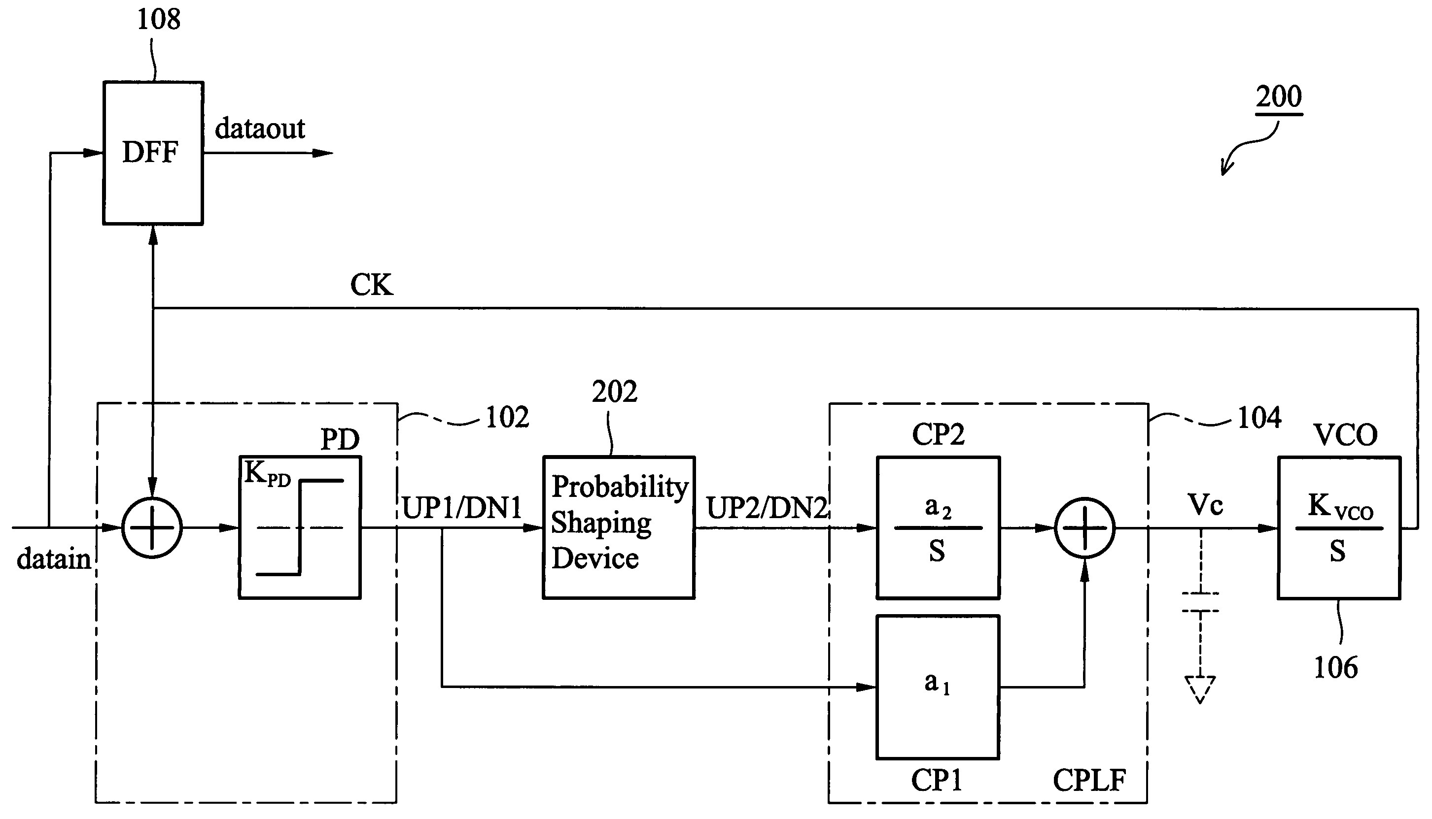
[0030]Please refer to FIG. 1 to consider influence on the CPLF device 104 due to latency or delay. The CPLF device 104 comprises a proportional path CP1 and integration path CP2 with functions or characteristics described as transfer functions of a1 and a2 / S respectively, wherein a1 and a2 are constants. Assuming that operating frequency is ω, the amplitude of the output signal of the CPLF device 104 is equal to 1, and ω=10ωz, ω=0.01ω0, here ω0 is the frequency of the clock signal CK.
[0031]Assume latency or delay is 5 clocks for example. Thus the phase lag is
[0032]θ=ωω0·5·2π=18°.
The transfer function of the CPLF device 104 is
[0033]a1+a2S=a2S(Sωz+1)=a2S(jωωz+1).
As...
PUM
 Abstract
Description
Claims
Application Information