Amplitude modulation driver

a driver and amplitude technology, applied in the field of modulation, can solve the problems of undesirable amount of electron tunneling and/or positive charge holing, transistor device “break down” or fail, etc., and achieve the effect of increasing voltage drop and higher tolerance to voltage fluctuations

Active Publication Date: 2009-08-18
PANASONIC CORP
View PDF3 Cites 4 Cited by
  • Summary
  • Abstract
  • Description
  • Claims
  • Application Information

AI Technical Summary

Benefits of technology

[0007]Preferably, the circuit is coupled to a transceiver that includes an amplitude modulator, an envelope modulator, and a power amplifier. The transceiver of some embodiments further includes a phase modulator, such that the transceiver is a polar transceiver. Typically, the first semiconductor device has a larger voltage drop than the second semiconductor device. The first semiconductor device also generally has a higher tolerance to voltage fluctuations. The first gate region often comprises a polycrystalline silicon material. The first semiconductor device is usually an NMOS type semiconductor device.
[0008]In some implementations, a drain lead of the first semiconductor device is coupled to an input voltage, a source lead of the first semiconductor device is coupled to a drain lead of the second semiconductor device, and a drain lead of the second semiconductor device is coupled to a low voltage, such that the first semiconductor device and the second semiconductor device are stacked.

Problems solved by technology

During these higher voltage conditions, the properties of the P-N junction change such that the transistor device “breaks down” or fails in operation.
For example, the increased voltage causes an undesirable amount of electron tunneling and / or positive charge holing, across the P-N junction.

Method used


Image

  • Amplitude modulation driver
  • Amplitude modulation driver
  • Amplitude modulation driver

Examples


Embodiment Construction

[0017]In the following description, numerous details and alternatives are set forth for purpose of explanation. However, one of ordinary skill in the art will realize that the invention can be practiced without the use of these specific details. In other instances, well-known structures and devices are shown in block diagram form in order not to obscure the description of the invention with unnecessary detail.

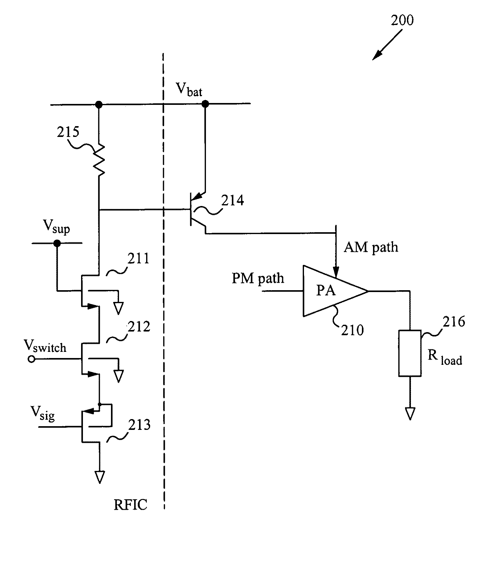
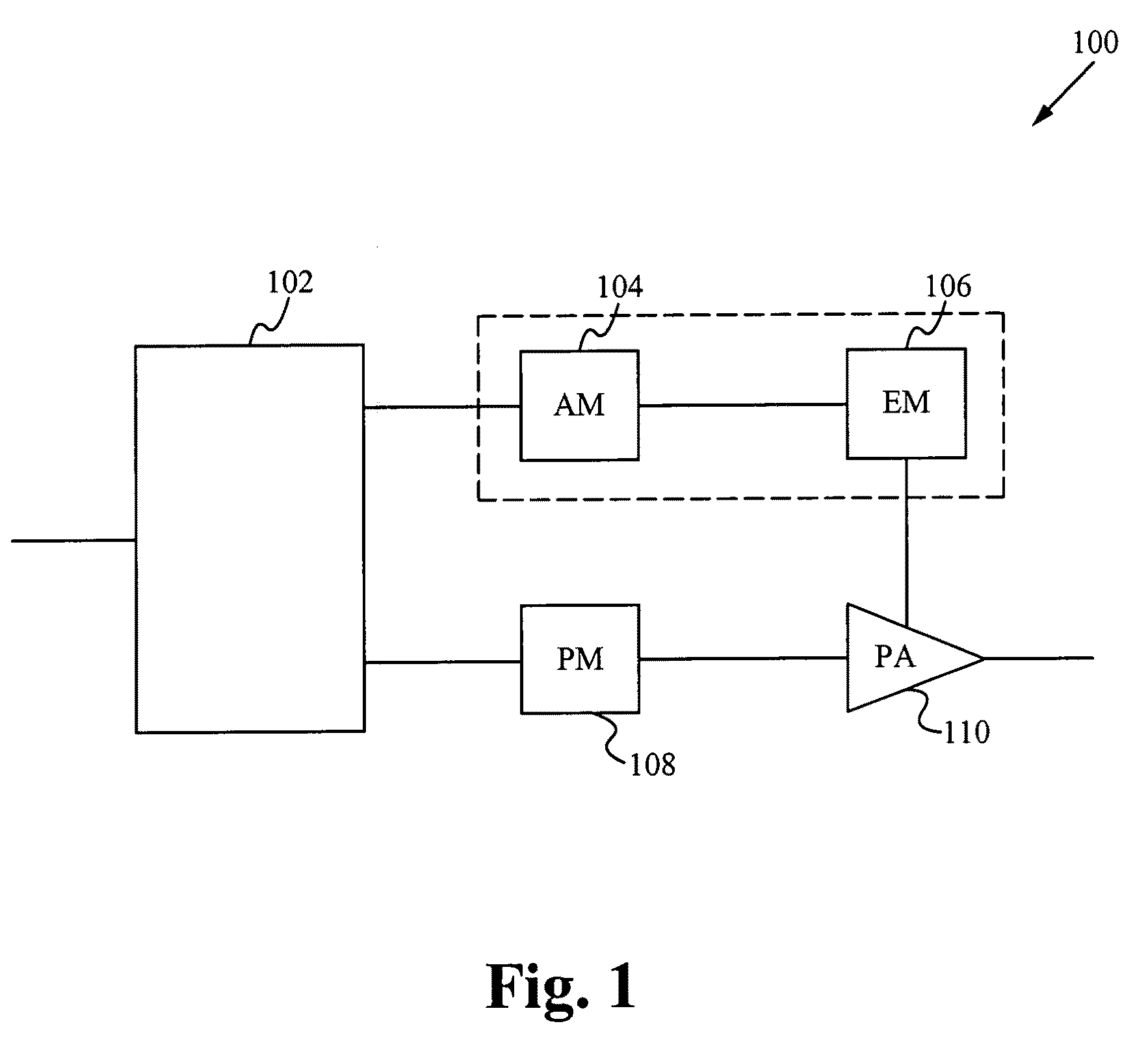
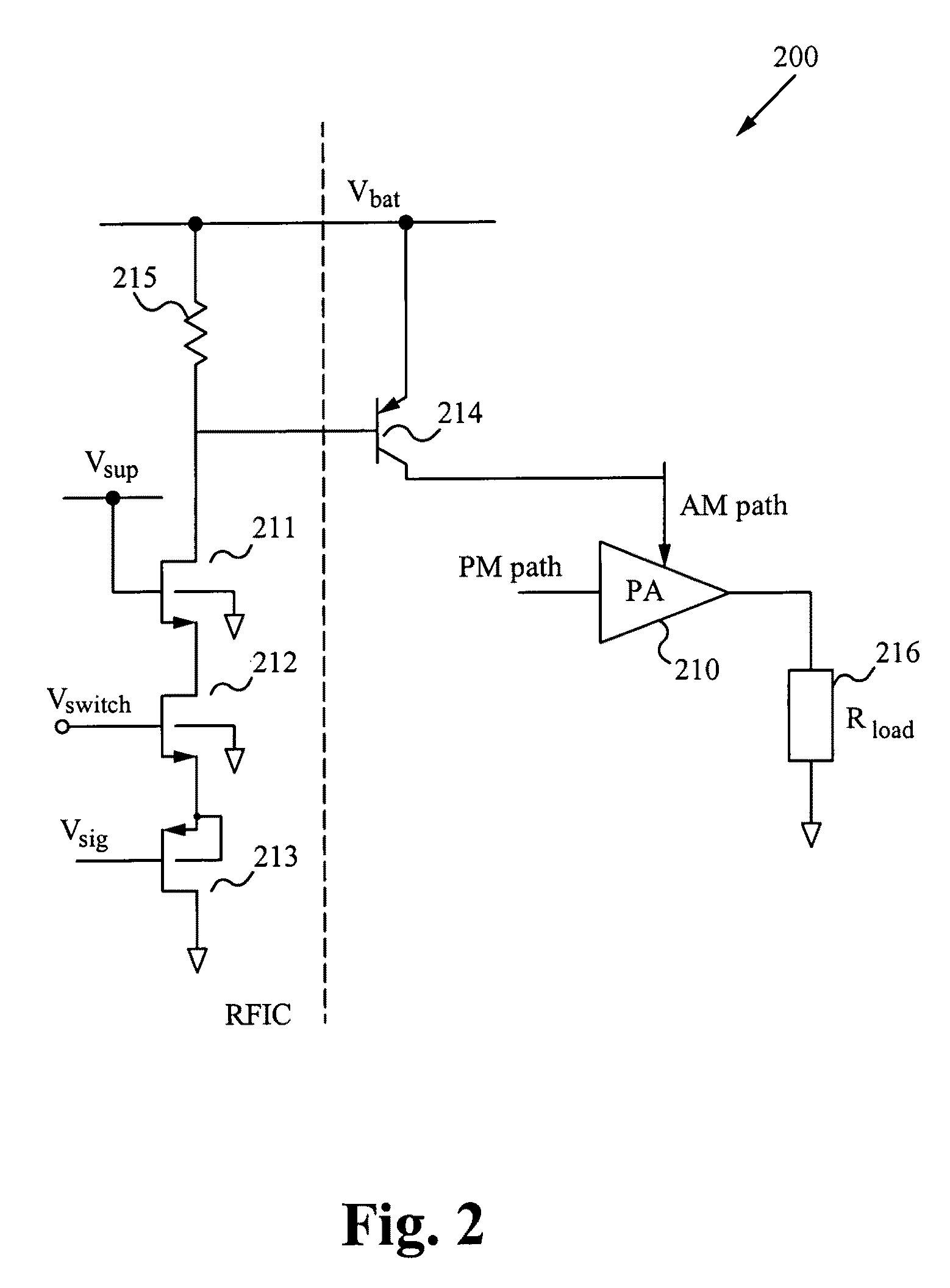
[0018]FIG. 1 illustrates a polar transmitter 100. As shown in this figure, the transmitter 100 includes an input signal module 102 coupled to an amplitude modulator 104. The amplitude modulator 104 is coupled in turn to an envelope modulator 106, which is coupled to a power amplifier 110. The input signal module 102 typically includes circuitry for the handling and / or conversion of a polar modulation signal, for example.

[0019]The input signal module 102 is also coupled to a phase modulator 108, which is coupled to the power amplifier 110. The path through the amplitude modulato...


PUM


Abstract

A circuit includes a first semiconductor device and a second semiconductor device. The first semiconductor device has a first source region, a first gate region, and a first drain region. The first gate region and the first drain region are separated by a first distance. The second semiconductor device has a second source region, a second gate region, and a second drain region. The second gate region and the second drain region separated by a second distance. The first distance is greater than the second distance.

Description

FIELD OF THE INVENTION[0001]The present invention generally relates to the field of modulation, and is more specifically directed to an amplitude modulation driver.BACKGROUND[0002]In recent years, researchers have proposed and implemented so called “polar” architectures for the improved transmission of signals. These polar architectures, rather than using complex In-phase Quadrature (IQ) components of a data signal, operate by using the polar coordinates of the data signal. Accordingly, polar implementations of modulation circuitry are used to transmit and receive voice and / or data in the radio frequency (RF) bands of the communications spectrum. Polar implementations have a number of advantages over their IQ-based counterparts.[0003]Regardless of implementation type, modern modulation circuits use transistor devices among their electronic components for the switching of electric current. These transistor devices include bipolar junction transistors (BJT), and metal oxide semiconduc...

Claims


Application Information

Patent Timeline
Patent Type & Authority Patents(United States)
IPC IPC(8): H03C3/38
CPCH03C5/00
Inventor OSMAN, SALEHDE LA CRUZ, DARWIN
Owner PANASONIC CORP
Why Eureka
Try Eureka