Microcomputer logic development device

a logic development and microcomputer technology, applied in the direction of electric control, machines/engines, instruments, etc., can solve the problem of no actual electronic control device, and achieve the effect of high speed, high performance ram monitor function, and high speed sampling ram monitoring

Inactive Publication Date: 2009-08-18
FUJITSU GENERAL LTD
View PDF12 Cites 4 Cited by
  • Summary
  • Abstract
  • Description
  • Claims
  • Application Information

AI Technical Summary

Benefits of technology

[0021]Therefore, the present invention provides a RAM measurement device comprised of a first block providing functions corresponding to a microcomputer core, a second block providing functions corresponding to microcomputer resources, a bus connecting the first and second blocks, and a RAM measurement block including a common memory and connecting the first block with a RAM measurement device. The processing for monitoring the RAM of the first block by the RAM measurement device is divided into processing for writing content of the RAM in the common memory and processing for sending content of the common memory to the RAM measurement device, and separating the processing timings. Due to this, an overall high speed, high performance RAM monitor function is realized.
[0022]According to the present invention, it is possible to provide a microcomputer logic development device realizing high speed sampling RAM monitoring by connecting an existing RAM measurement device. Due to this, it is possible to improve the logic development environment. Further, it is possible to utilizing existing devices as they are and to reduce costs.

Problems solved by technology

However, at the time of development of advance logic, there are no actual electronic control devices with the next generation microcomputers built in them.

Method used


Image

  • Microcomputer logic development device
  • Microcomputer logic development device
  • Microcomputer logic development device

Examples


Embodiment Construction

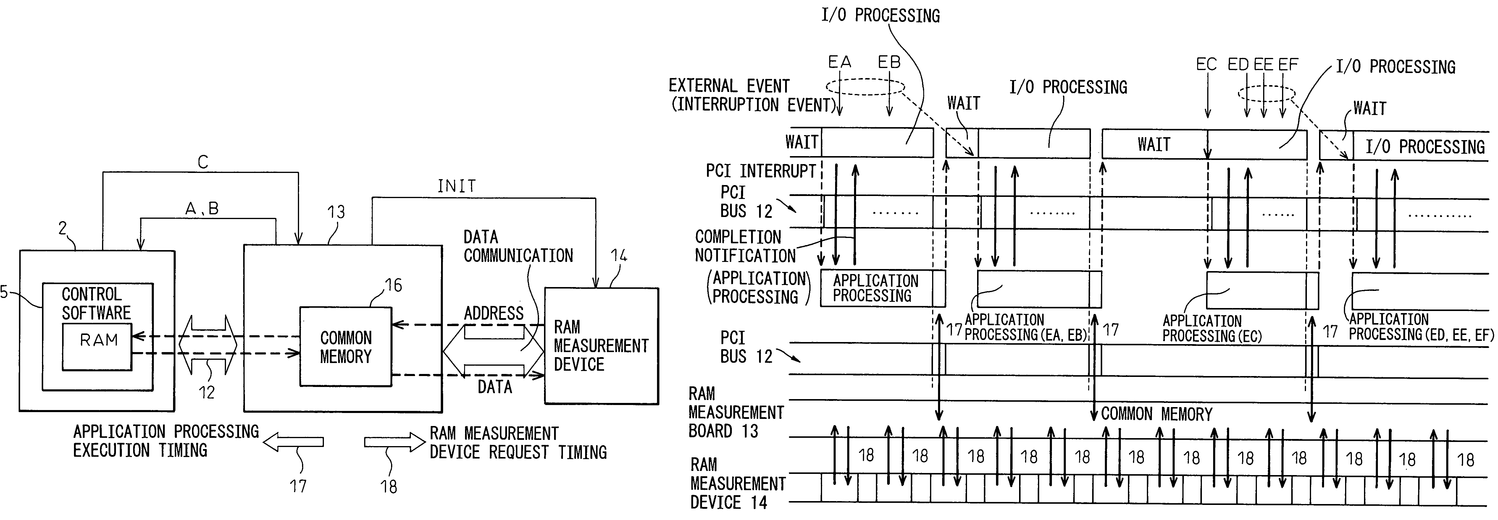
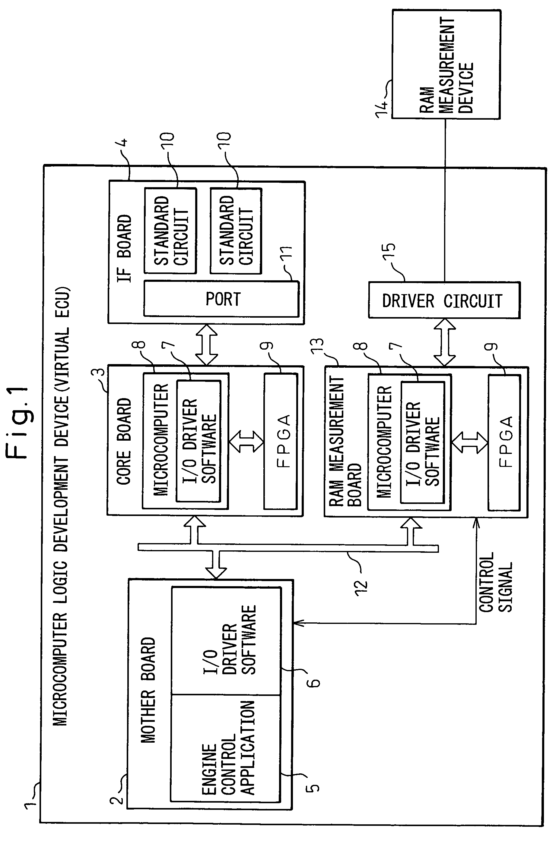
[0036]Preferred embodiments of the microcomputer logic development device to which the present invention is applied will be described in detail below while referring to the attached figures.

[0037]FIG. 1 shows the configuration of a microcomputer logic development device 1 which realizes a virtual ECU.

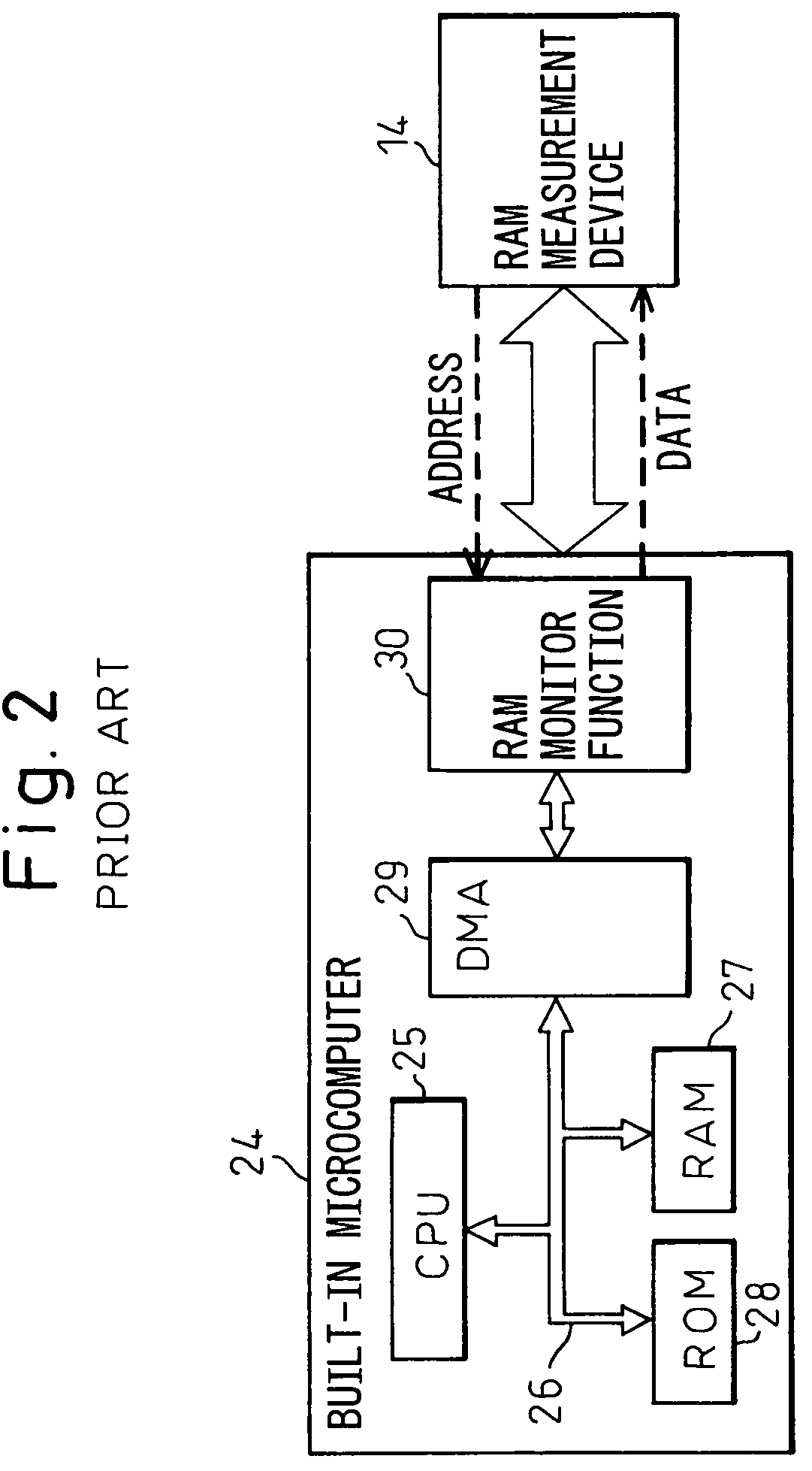
[0038]The microcomputer logic development device 1 is comprised of three boards, that is, a mother board 2 for realizing functions corresponding to a microcomputer, a core board 3 for realizing functions corresponding to microcomputer resources, and an interface board for realizing functions corresponding to ECU hardware. Their configurations are similar to those described in the above patent publications.

[0039]As the processing device built in the mother board 2, a general use CPU is used. This CPU processing performance is set with several levels better processing performance than that actually used for the built-in microcomputer. The microcomputer is loaded with an engine control app...


PUM


Abstract

A microcomputer logic development device realizing high speed sampling RAM monitoring by connecting an existing RAM measurement device, provided with a first block providing functions corresponding to a microcomputer core, a second block having functions corresponding to microcomputer resources, a bus connecting the first and second blocks, and a RAM measurement block provided with a common memory, connected with the bus and RAM measurement device, and realizing a RAM monitor function with respect to the first block, the RAM measurement block realizing a high speed RAM monitoring operation by dividing the timing for processing between the first block and common memory and the timing for processing between the common memory and RAM measurement device.

Description

[0001]This application claims priority to Japanese Patent Application No. JP-2003-191940 filed on Jul. 4, 2003.BACKGROUND OF THE INVENTION[0002]1. Field of the Invention[0003]The present invention relates to a microcomputer logic development device used when developing a built-in microcomputer, more particularly relates to a microcomputer logic development device adding a RAM monitor function.[0004]2. Description of the Related Art[0005]Electronic control units (ECU) for engine control and other electronic control devices have to be improved in performance along with enactment of tougher emission controls and other legal regulations and improvements in microcomputer performance. Therefore, electronic control devices have to be improved every year. New applications are being developed in advance of current levels of electronic control device performance (hereinafter called “advance logic”).[0006]Such advance logic is often developed targeting the next generation of microcomputers off...

Claims


Application Information

Patent Timeline
Patent Type & Authority Patents(United States)
IPC IPC(8): G06F9/455G06F11/00F02D45/00G06F9/44G06F11/22G06F11/28G06F11/30G06F13/10G06F13/12G06F17/50
CPCG06F17/5022G06F30/33
Inventor IMADA, SHOUGOKANOU, KOUICHIHIGUCHI, TAKASHI
Owner FUJITSU GENERAL LTD
Why Eureka
Try Eureka