Current controlling circuit arrangement and associated method for reducing crosstalk

a current control circuit and crosstalk technology, applied in the field of circuit arrangement, can solve the problems of undesirable crosstalk from interference on power supply systems between function groups which are monolithically integrated together, more or less pronounced transient coupling between load connection connections, and undesirable crosstalk from signals or interference on supply voltages

Inactive Publication Date: 2009-08-25
INFINEON TECH AG
View PDF11 Cites 1 Cited by
  • Summary
  • Abstract
  • Description
  • Claims
  • Application Information

AI Technical Summary

Benefits of technology

[0011]Advantageously, the control means preferably comprises a control capacitor which is coupled between the control input of the controlled current source and the input connection of the circuit arrangement. The control capacitor is a simple way of providing a control signal for the controlled current source. It is thus possible, with particularly little complexity, for the controlled current source to produce a current which corresponds to the average current drawn by the load impedance.
[0022]To facilitate a speedy transient process at the same time, there is preferably a further differential amplifier. The first and second inputs of the further differential amplifier are respectively connected to the first and second inputs of the differential amplifier. The output of the further differential amplifier is connected to the control input of the controlled current source via a switch. The switch can therefore be closed in order to provide a speedy transient process and can be opened again when the transient process has finished. This means that the advantage of rapid settling is associated with a broadband blocking action after the switch has been opened.
[0026]Preferably, a plurality of circuit arrangements are provided on a chip and are associated with respective load impedances. In this manner, the load impedances can be operated at different and / or the same supply voltages and undesirable radiated interference from transient radio-frequency interference on the common substrate can be suppressed.
[0027]One or more aspects of the present invention significantly reduce crosstalk by providing not a passive but rather an active measure to reduce crosstalk effects via the supply voltage. This is done by controlling the current flowing through the load impedance such that the current corresponds to an average current drawn by the load impedance.

Problems solved by technology

In integrated semiconductor circuits, crosstalk from interference on power supply systems between function groups which are monolithically integrated together is undesirable.
Voltage drops across bonding wires and voltage drops across parasitic series inductances in the power supply line as a result of high-frequency and very high-frequency fluctuations in the current carried by on-chip loads cannot be compensated for by a backup capacitor on the board which stabilizes the supply voltage.
Since integrated structures have parasitic connections to the silicon substrate, it becomes clear that relatively high-frequency transient dynamic load changes in integrated loads result in more or less pronounced transient couplings between the connections of the loads.
This means that there is undesirable crosstalk from signals or interference on supply voltages.

Method used


Image

  • Current controlling circuit arrangement and associated method for reducing crosstalk
  • Current controlling circuit arrangement and associated method for reducing crosstalk
  • Current controlling circuit arrangement and associated method for reducing crosstalk

Examples


Embodiment Construction

[0044]One or more aspects of the present invention will now be described with reference to the drawing figures, wherein like reference numerals are used to refer to like elements throughout. It should be understood that the drawing figures and following descriptions are merely illustrative and that they should not be taken in a limiting sense. In the following description, for purposes of explanation, numerous specific details are set forth in order to provide a thorough understanding of the present invention. It will be evident to one skilled in the art, however, that the present invention may be practiced without these specific details. Thus, it will be appreciated that variations of the illustrated systems and methods apart from those illustrated and described herein may exist and that such variations are deemed as falling within the scope of the present invention and the appended claims.

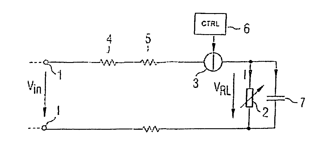
[0045]FIG. 1 illustrates a circuit arrangement according to one or more aspects of the presen...


PUM


Abstract

A circuit arrangement and associated method for reducing crosstalk are disclosed. A load impedance is connected via a controlled current source to an input connection for supplying a supply voltage (Vin) in the circuit arrangement. The current source is actuated using a control means such that the current source outputs a current which corresponds to the average current drawn by the load impedance. In this manner, merely a small voltage drop occurs on the supply voltage while radio-frequency interference is concurrently mitigated.

Description

REFERENCE TO RELATED APPLICATIONS[0001]This application claims the benefit of the priority date of German application DE 10 2004 010 169.8, filed on Mar. 2, 2004, the contents of which are herein incorporated by reference in their entirety.FIELD OF THE INVENTION[0002]The present invention relates to a circuit arrangement, the use thereof on a chip and a method for reducing crosstalk.BACKGROUND OF THE INVENTION[0003]In integrated semiconductor circuits, crosstalk from interference on power supply systems between function groups which are monolithically integrated together is undesirable. To reduce crosstalk effects via power supply systems, it is normal practice to take passive measures. One such measure is capacitive backup of the supply voltage, for example.[0004]Voltage drops across bonding wires and voltage drops across parasitic series inductances in the power supply line as a result of high-frequency and very high-frequency fluctuations in the current carried by on-chip loads c...

Claims


Application Information

Patent Timeline
Patent Type & Authority Patents(United States)
IPC IPC(8): G05F1/00G05F1/70H01L23/66
CPCG06F1/26H01L23/50H01L2924/0002H01L2924/00
Inventor OEHM, JUERGEN
Owner INFINEON TECH AG
Why Eureka
Try Eureka