Thin film capacitor element composition, high permittivity insulation film, thin film capacitor element, thin film multilayer capacitor, and method of production of thin film capacitor element

a technology capacitor elements, applied in the direction of fixed capacitors, thin/thick film capacitors, ceramics, etc., can solve the problems of obstructing the realization of ultra-high integrated circuits, delay in reducing the size of thin film capacitors, slow film reduction, etc., to achieve superior frequency characteristic, bias characteristic, and c-axis orientation high, the effect of improving the quality of the capacitor

Active Publication Date: 2009-08-25
TDK CORPARATION
View PDF25 Cites 20 Cited by
  • Summary
  • Abstract
  • Description
  • Claims
  • Application Information

AI Technical Summary

Benefits of technology

[0070]According to the present invention, a thin film capacitor element composition high in c-axis orientation, in particular low in Curie point, and superior in frequency characteristic, bias characteristic, and dielectric loss or other electrical characteristics and a high permittivity insulation film, thin film capacitor element, thin film multilayer capacitor, and method of production of a thin film capacitor element using the same can be provided. Further, in the present invention, in particular by formation by the solution method, a thin film capacitor element having a dielectric thin film high in c-axis orientation, in particular low in Curie point and superior in electrical characteristics, can be easily produced.

Problems solved by technology

For example, thin film capacitors using single layer of dielectric thin film have been slow in being reduced in size in integrated circuits with transistors and other active elements and have become factors obstructing the realization of ultra-high integrated circuits.
The delay in reducing the size of thin film capacitors is due to the low permittivity of the dielectric materials used for them.
Further, in recent years, from the viewpoint of the capacitance density, the conventional SiO2 and Si3N4 multilayer films are no longer sufficient for the capacitor materials for the next generation DRAMs (Gigabit generation), and material systems with higher permittivity have gathered attention.
However, when using this type of dielectric material, the reduction in thickness of the dielectric film leads to a drop in the permittivity.
Further, reduction in thickness leads to the formation of holes in the dielectric film and thereby deterioration of the leakage characteristic and withstand voltage.
Further, the formed dielectric film tends to be poor in surface flatness and poor in rate of change of the permittivity with respect to temperature.
However, for example, when using the sheet method (method of using a dielectric layer paste to form a dielectric green sheet layer on a carrier film by the doctor blade method etc., printing an internal electrode layer paste over this in a predetermined pattern, then peeling off and stacking one layer at a time) to produce a multilayer ceramic capacitor, the dielectric layers cannot be formed thinner than the ceramic material powder.
Further, due to short-circuits caused by defects in the dielectric layers, breakage of the internal electrodes, or other problems, it has been difficult to reduce the dielectric layers in thickness to for example 2 μm or less.
Further, when reducing the thickness of each of the dielectric layer, there were also limits to the number of layers.
Note that there are similar problems when using the printing method (for example, the method of using the screen printing method to alternately print dielectric layer paste and internal electrode layer paste on a carrier film a plurality of times, then peeling off the carrier film) to produce a multilayer ceramic capacitor.
However, the dielectric thin films formed by the methods described in these publications are poor in surface flatness and, when overly stacked, suffer from electrode short-circuiting.
Due to this, it was only possible to produce devices with at the most 12 to 13 layers.
For this reason, even if the capacitor could be reduced in size, a higher capacitance could not be achieved.
However, this publication did not disclose anything at all regarding under what conditions (for example, the relationship between the surface of the substrate and the c-axis orientation of the compound) the thickness is reduced (for example 1 μm or less) is it possible to obtain a relatively high permittivity and low loss even when thin and whether a thin film superior in leakage characteristic, improved in withstand voltage, superior in temperature characteristic of the permittivity, and superior in surface flatness can be obtained.
Further, with the methods of production of the bismuth layered compound dielectric materials described in these publications (for example, MOCVD and single crystal growth), introduction of lanthanum (rare earth element) in a content of more than that described in the publications is difficult.

Method used


Image

  • Thin film capacitor element composition, high permittivity insulation film, thin film capacitor element, thin film multilayer capacitor, and method of production of thin film capacitor element
  • Thin film capacitor element composition, high permittivity insulation film, thin film capacitor element, thin film multilayer capacitor, and method of production of thin film capacitor element
  • Thin film capacitor element composition, high permittivity insulation film, thin film capacitor element, thin film multilayer capacitor, and method of production of thin film capacitor element

Examples


first embodiment

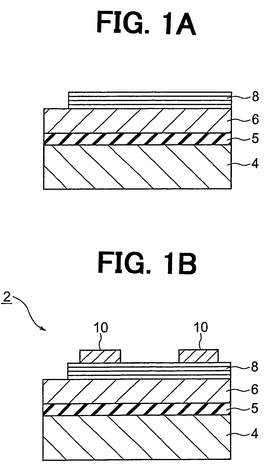
[0083]In this embodiment, as the thin film capacitor element, a thin film capacitor forming a dielectric thin film by a single layer will be used as an example for the explanation.

[0084]As shown in FIG. 1A and FIG. 1B, the thin film capacitor 2 according to an embodiment of the present invention has a substrate 4 and a lower portion electrode thin film 6 over this substrate 4 through an insulation layer 5. The lower portion electrode thin film 6 is formed over it with a dielectric thin film 8. The dielectric thin film 8 is formed over it with an upper portion electrode thin film 10. Note that in this embodiment, an insulation layer 5 is preferably formed over the substrate 4, but there is no absolute need to form the insulation layer 5. For example, the substrate 4 may have the lower portion electrode thin film 6 directly formed over it.

[0085]The substrate 4 and insulation layer 5 are not particularly limited, but are comprised of a good lattice matching single crystal (for example,...

second embodiment

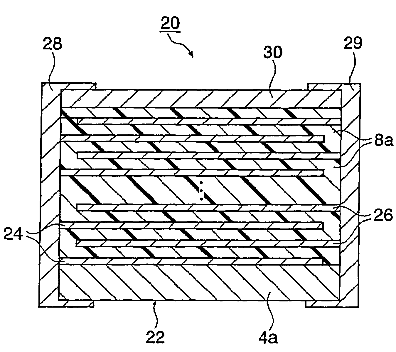
[0125]In the present embodiment, as the thin film capacitor element, a thin film multilayer capacitor formed with multiple layers of dielectric thin film is explained as an example.

[0126]As shown in FIG. 3, the thin film multilayer capacitor 20 according to an embodiment of the present invention has a capacitor body 22. The capacitor body 22 is comprised of a substrate 4a on which a dielectric thin film 8a and internal electrode thin films 24, 26 are alternately stacked in a plurality of layers and further formed with a protective layer 30 so as to cover the dielectric thin film 8a positioned at the outermost part thereby forming a multilayer structure. The capacitor body 22 is formed at its two ends with a pair of external electrodes 28 and 29. The pair of external electrodes 28, 29 are electrically connected to the exposed end faces of the internal electrode thin films 24, 26 alternately arranged inside the capacitor body 22 to form a capacitor circuit. The capacitor body 22 is no...

example 1

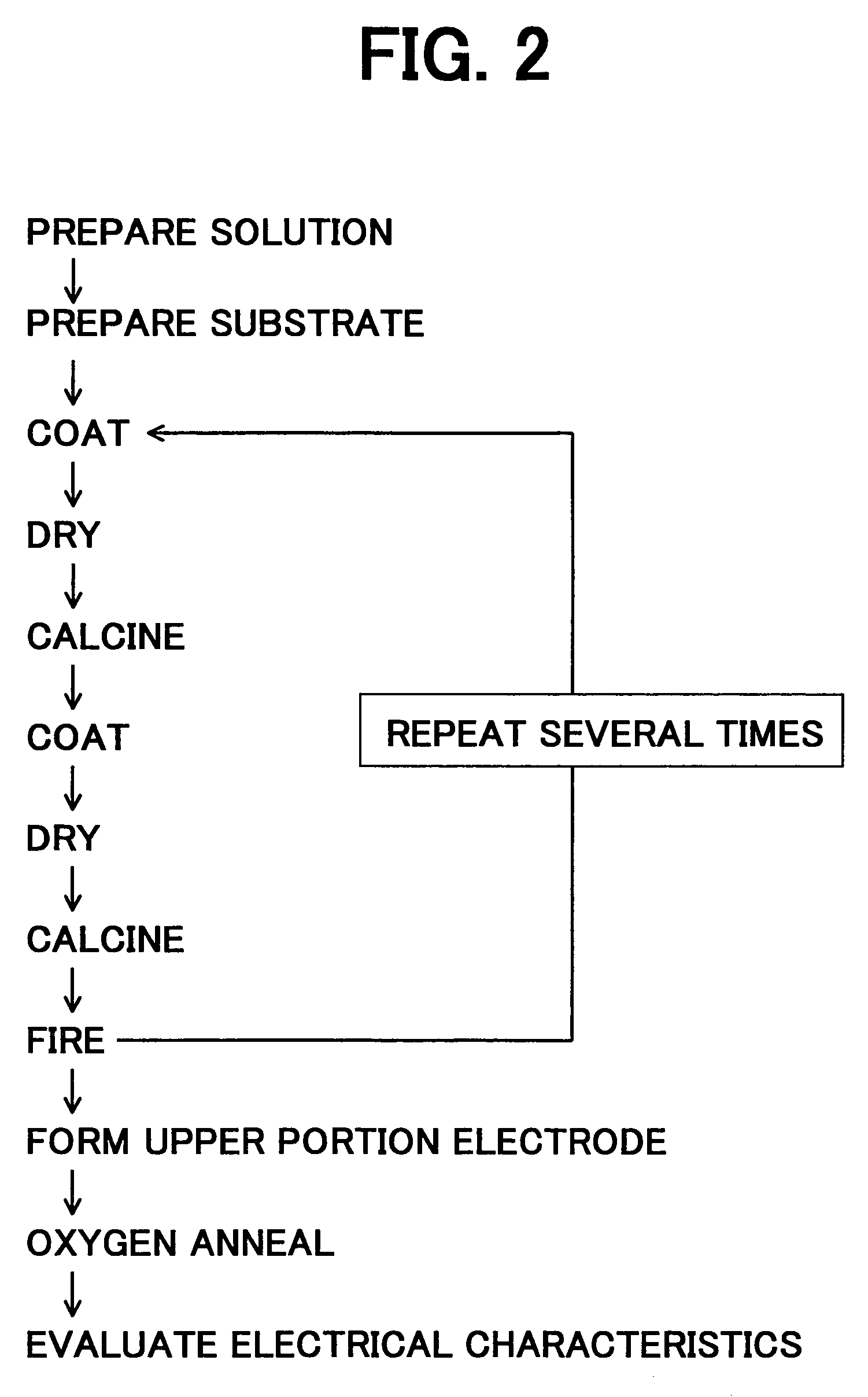
[0134]As shown in FIG. 2, first, the stock solutions for forming the dielectric thin film 8 shown in FIG. 1A were prepared. In this example, the solutions shown below were prepared for making the dielectric thin film 8 a bismuth layered compound expressed by the stoichiochemical formula Bi4−xLaxTi3O12.

[0135]First, bismuth 2-ethylhexanoate in a 2-ethylhexanoic acid solution and titanium 2-ethylhexanoate and lanthanum 2-ethylhexanoate in a toluene solution were prepared.

[0136]Next, the bismuth 2-ethylhexanoate in an amount of 4−x moles, the titanium 2-ethylhexanoate in an amount of 3 moles, and the lanthanum 2-ethylhexanoate in an amount of x (x=0, 1.0, 1.1, 1.25, 1.5, and 2.0) moles were mixed to obtain several types of mixed solutions. Note that bismuth 2-ethylhexanoate was added in 10 to 20 mol % excess with respect to the amount of moles when using the stoichiochemical ratio for mixture.

[0137]Next, the mixed solutions were diluted by toluene to, converted to Bi4−xLaxTi3O12, 0.1 mo...


PUM

PropertyMeasurementUnit
thicknessaaaaaaaaaa
temperatureaaaaaaaaaa

Abstract

A thin film capacitor element composition having a bismuth layered compound with a c-axis oriented substantially vertical to the substrate surface, wherein the bismuth layered compound is expressed by the formula (Bi2O2)2+(Am−1BmO3m+1)2− or Bi2Am−1BmO3M+3, the symbol m in the formula is an odd number, at least part of the Bi and / or A of the bismuth layered compound is substituted by a rare earth element, and the number of moles substituted by the rare earth element is larger than 1.0 and 2.8 or less with respect to the number of moles (m+1) of the total of Bi and A.

Description

TECHNICAL FIELD[0001]The present invention relates to a thin film capacitor element composition, high permittivity insulation film, thin film capacitor element, thin film multilayer capacitor, and method of production of a thin film capacitor element.BACKGROUND ART[0002]In recent years, in the field of electronic devices, the higher densities and higher integration degrees of electronic circuits have led to a demand for further reductions in size and improvements in the performance of capacitor element as an essential circuit element in a variety of electronic circuits.[0003]For example, thin film capacitors using single layer of dielectric thin film have been slow in being reduced in size in integrated circuits with transistors and other active elements and have become factors obstructing the realization of ultra-high integrated circuits. The delay in reducing the size of thin film capacitors is due to the low permittivity of the dielectric materials used for them. Therefore, to re...

Claims


Application Information

Patent Timeline
Patent Type & Authority Patents(United States)
IPC IPC(8): H01G4/06C04B35/462C04B35/47C04B35/475C04B35/495C04B35/622H01B3/12H01G4/12H01G4/33
CPCC04B35/462C04B35/475H01G4/1209H01G4/33C04B35/47Y10T29/435C04B2235/3213C04B2235/3227C04B2235/3298C04B2235/441C04B2235/656C04B2235/6562C04B2235/6565C04B2235/6567C04B2235/787
Inventor SAKASHITA, YUKIO
Owner TDK CORPARATION
Why Eureka
Try Eureka