Bottom entry interconnection element for connecting components to a circuit board

a technology of interconnection elements and components, which is applied in the direction of coupling contact members, fixed connections, coupling device connections, etc., can solve the problems of inefficiency in board fabrication and manufacturing, the amount of space that each board occupies, and the increase of costs

Active Publication Date: 2009-09-01
PROCOMM INT PTE LTD
View PDF40 Cites 67 Cited by
  • Summary
  • Abstract
  • Description
  • Claims
  • Application Information

AI Technical Summary

Problems solved by technology

One particular constraint in system design and manufacturing of such boards is the amount of space that each board has to handle the various components and modules.
This arrangement often leads to difficulties and inefficiencies in board fabrication and manufacturing and thus can lead to higher costs.
The hand soldering is very difficult due to the large mass presented by the leads 14 of the power converter module 12, as well as the extensive external and internal power planes that typically exist on the circuit board 10.
However, these machines are not standard equipment items in board manufacturing shops and rework / repair facilities, are very high capital expense items, and still experience similar solder difficulties as manual soldering due to the large mass of leads and extensive power planes on the circuit board.
This problem is further compounded by the fact that the power converter module has internal solder connections that are at risk of solder re-reflow, and subsequent damage, when the external leads 14 are manually soldered to the circuit board.
As a result, the risk of internal damage requires each power converter module manufacturer to stipulate strict manual solder parameters (e.g., temperature and solder iron dwell time applied to each lead).
Such parameters are extremely difficult to adhere to.
Still further, the recent introduction of lead-free solder alloys (RoHS regulations) results in still greater difficulty with manual soldering.
This is because lead-free solders have much higher melting temperatures than traditional lead-based alloys and thus do not “wet” as easily.
Furthermore, the periodic need to remove a soldered power converter module (such as for rework or repair) is extremely difficult, and often results in irreparable damage to the circuit board and / or the module.
However, the existing and commercially available through-hole socket arrangements and components have significant drawbacks.
Such extra assembly processes or manual processes inevitably result in higher assembly costs and / or inferior attachment quality (including inferior long-term reliability) of the components or modules to the board.
A further complication is that many commercially available off-the-shelf power sockets that have a discrete design are not suitable for the vacuum pickup that is used in automated pick-and-place techniques using standard surface-mount assembly equipment.
This results in additional capital costs.
Hand placement, on the other hand, is inferior in both cost and quality, as compared to viable automated placement alternatives.
The tolerance requirements make it infeasible to use automated insertion techniques with standard assembly equipment.
This further dictates that manual placement be used, resulting in higher assembly costs.
Additionally, the reliability of the solder joint is compromised, per electronics industry end point requirements, because the tight clearance between the socket and board hole does not provide sufficient space for the proper flow of solder.
These sockets do not have ability to properly mate and provide proper contact force for pins of power converters which have high positional tolerance.
Additionally, this ganged approach is cost prohibitive for small to moderate volumes of different power converter module designs that have different pin arrangements.

Method used


Image

  • Bottom entry interconnection element for connecting components to a circuit board
  • Bottom entry interconnection element for connecting components to a circuit board
  • Bottom entry interconnection element for connecting components to a circuit board

Examples


Embodiment Construction

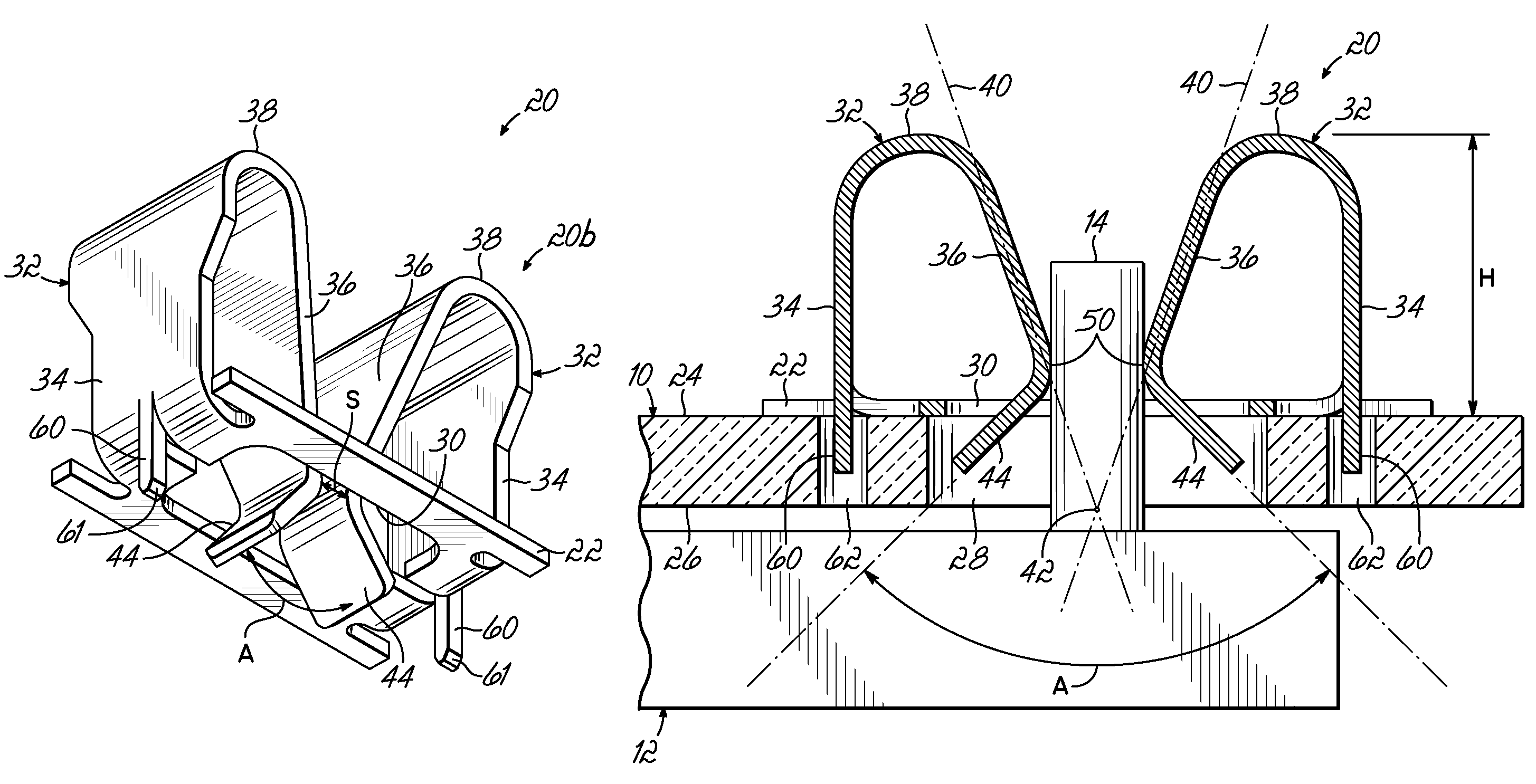
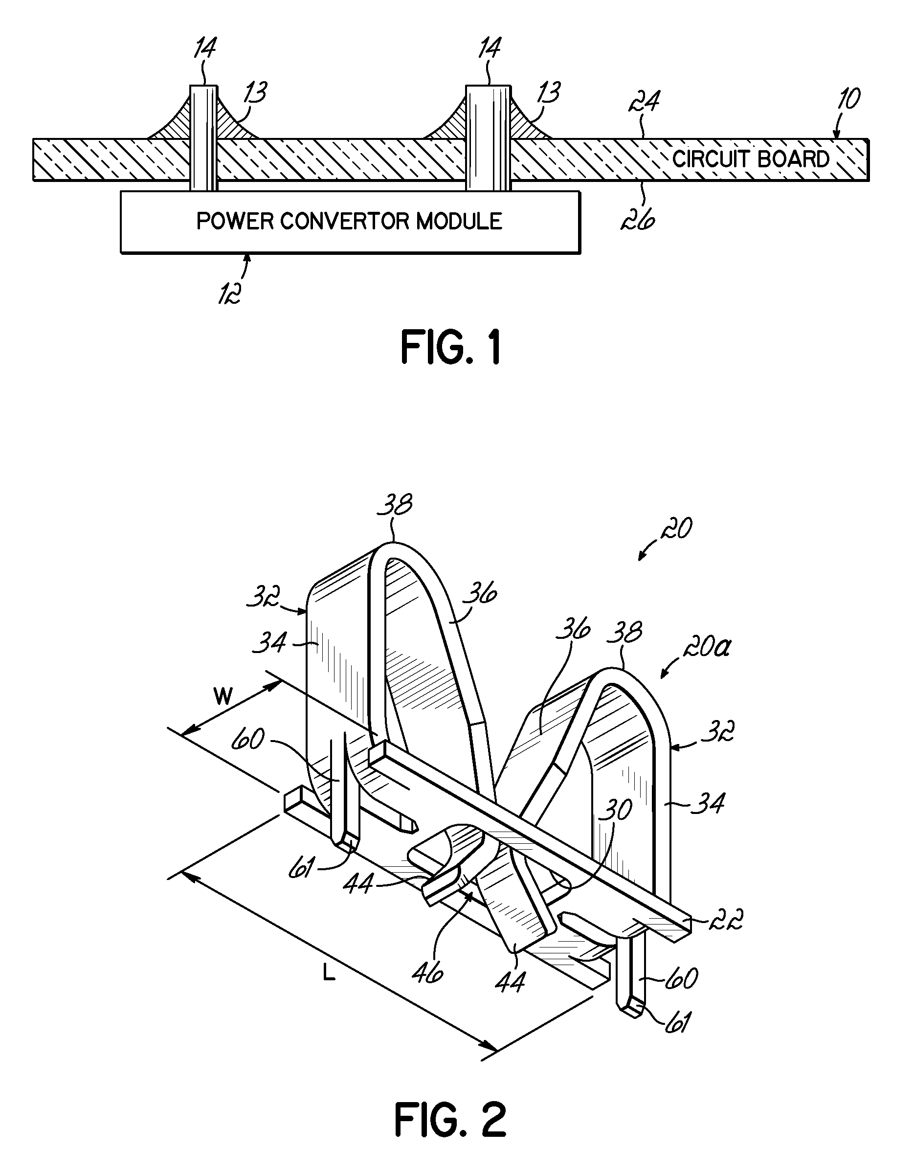
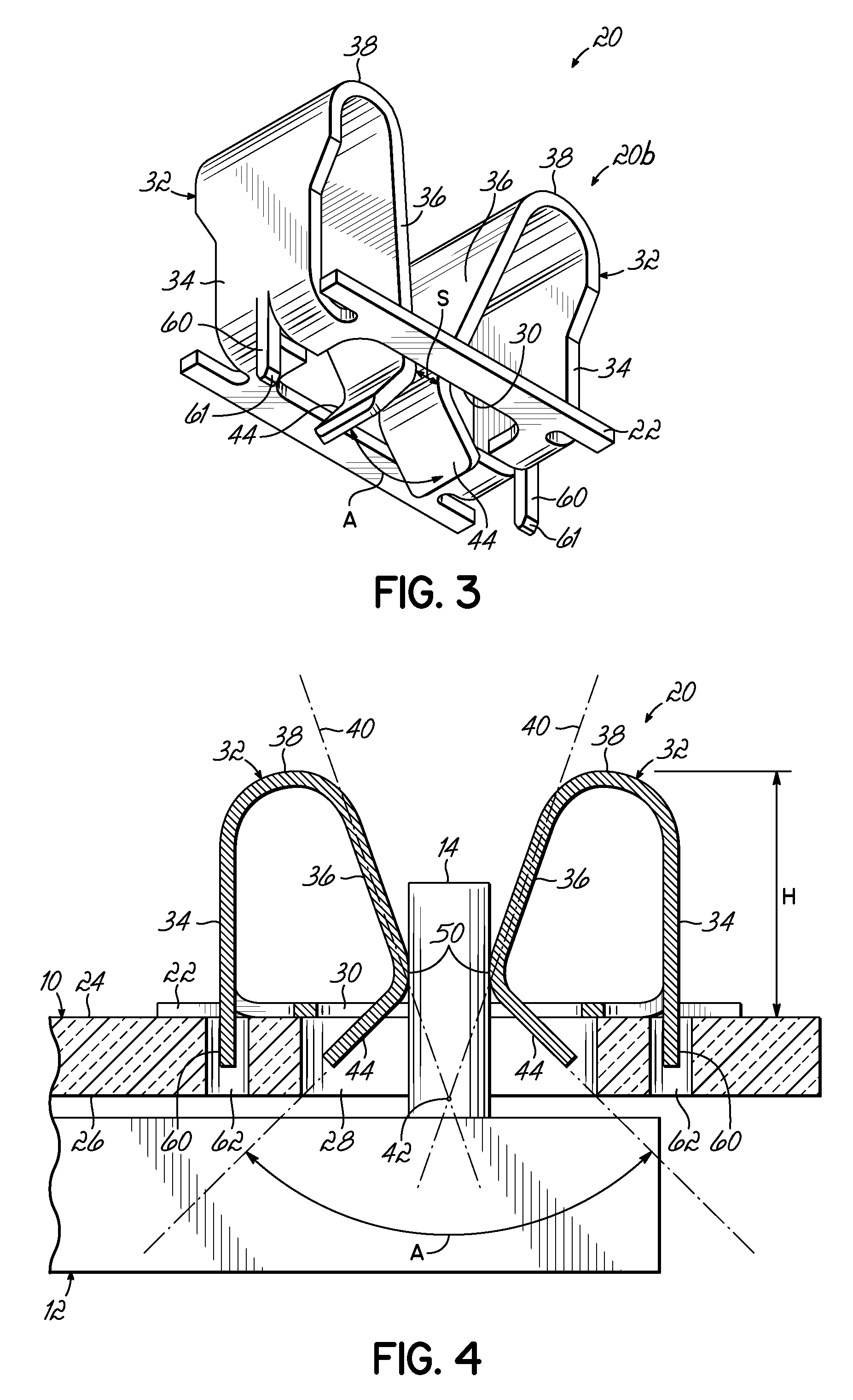
[0023]The present invention can address various drawbacks in the prior art as noted above, and provides an interconnection element or socket to couple a component to a circuit board. It provides a robust mechanical and electrical connection between a circuit board and one or more components or modules, such as a power converter module. The interconnection element provides both surface-mount technology (SMT) and through-hole attachment techniques, thus, providing a robust physical attachment as well as a robust electrical connection between the board and component. The interconnection elements are discrete to adapt to various different component lead or pin arrangements, and do not require precise pin alignment with the interconnection element.

[0024]The present invention provides a top side interconnection element that is configured to receive pins or leads from components inserted on the bottom side of a circuit board. The invention is configured for automated surface-mount technolo...


PUM


Abstract

An interconnection element for coupling a component with a circuit board having a top side and a bottom side has a planar portion configured to be surface mounted on the top side of the circuit board to overlie an opening in the circuit board. An opening is formed in the planar portion to coincide with the circuit board opening. Opposing spring fingers are coupled to the planar portion, and each spring finger has a gripping leg extending downwardly toward the planar portion. The gripping legs are positioned on opposite sides of the opening in the planar portion and extend through the opening in the planar portion to extend into the board opening and capture a component lead that extends in the board opening from the bottom side of the circuit board.

Description

FIELD OF THE INVENTION[0001]The present invention relates generally to the issue of coupling multiple circuit elements, components, or modules to a printed circuit board and more specifically to mounting a power converter module or other module to a circuit board.BACKGROUND OF THE INVENTION[0002]The circuit components and modules for various electronic systems, such as, for example, telecommunication systems and equipment, are often arranged and housed in the form of one or more printed circuit boards. The multiple electronic components or modules are mounted on the board, and conductive traces or patterns operably connect the components together. For example, the motherboard of an RF power amplifier, as used in telecommunication applications, will contain not only individual circuit components, but also must support one or more larger power converter modules for various power requirements on the motherboard. One particular constraint in system design and manufacturing of such board...

Claims


Application Information

Patent Timeline
Patent Type & Authority Patents(United States)
IPC IPC(8): H01R12/00
CPCH05K3/32H01R12/718H05K2201/10295H05K2201/10962H05K2201/1059H01R12/57H01R12/58
Inventor UPASANI, SANJAY SUDHAKARKEBEDE, SEBSIBEBROWN, RICHARD WILLIAMBERGMAN, SCOTT ALLEN
Owner PROCOMM INT PTE LTD
Why Eureka
Try Eureka