Nonvolatile memory devices having multi-filament variable resistivity memory cells therein

a memory cell and non-volatile technology, applied in the field of integrated circuit memory devices, can solve the problems of difficult transition from the reset state to the reset state or the transition from the reset state to the reset state, and achieve the effect of improving programming reliability

Inactive Publication Date: 2009-09-08
SAMSUNG ELECTRONICS CO LTD
View PDF13 Cites 11 Cited by
  • Summary
  • Abstract
  • Description
  • Claims
  • Application Information

AI Technical Summary

Benefits of technology

[0007]Embodiments of the present invention include non-volatile integrated circuit memory devices that utilize variable resistivity materials (e.g., perovskite materials) for data retention. According to some of these embodiments, a non-volatile memory device includes an array of memory cells having non-volatile data storage regions therein that are formed from multi-filament variable resistivity materials. To improve programming reliability, a filament-forming circuit is provided. This filament-forming circuit is electrically coupled to a terminal of the memory cell during a filament-forming operation. The filament-forming circuit is configured to drive the terminal with a monotonically increasing sequence of voltages (e.g., filament-forming voltages) that operate to form filaments within the variable resistivity material during the filament-forming operation. This monotonically increasing sequence may be a stair-step sequence or a linear ramp-shaped sequence, for example.

Problems solved by technology

Since the filament-forming voltage may be a relatively high level, the variable resistive material 2 may be partially broken down, or the filaments may be formed to be excessively thick such that transition from the reset state to the set state or transition from the set state to the reset state can become difficult.

Method used


Image

  • Nonvolatile memory devices having multi-filament variable resistivity memory cells therein
  • Nonvolatile memory devices having multi-filament variable resistivity memory cells therein
  • Nonvolatile memory devices having multi-filament variable resistivity memory cells therein

Examples


Embodiment Construction

[0022]Advantages and features of the present invention and methods of accomplishing the same may be understood more readily by reference to the following detailed description of preferred embodiments and the accompanying drawings. The present invention may, however, be embodied in many different forms and should not be construed as being limited to the embodiments set forth herein. Rather, these embodiments are provided so that this disclosure will be thorough and complete and will fully convey the concept of the invention to those skilled in the art, and the present invention will only be defined by the appended claims. Like reference numerals refer to like elements throughout the specification.

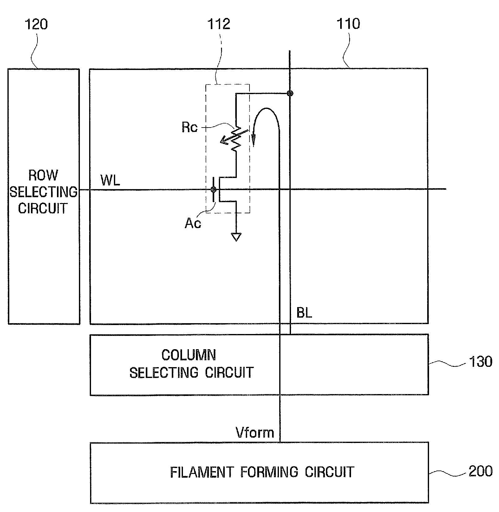
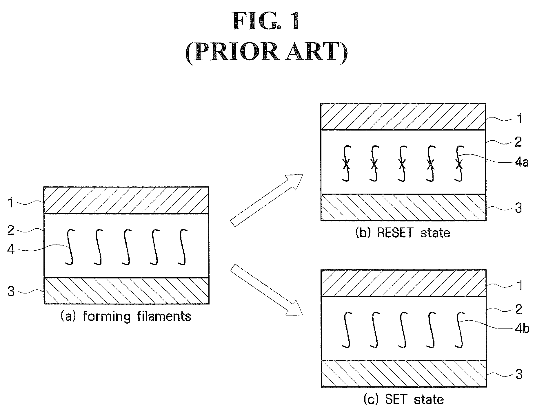
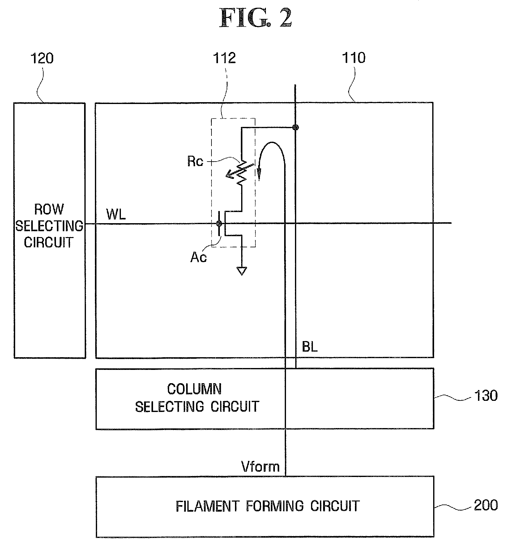
[0023]The present invention will now be described more fully with reference to the accompanying drawings, in which preferred embodiments of the invention are shown. Hereinafter, the exemplary embodiments of the invention will be described below using a resistive RAM (RRAM). However, it will ...


PUM


Abstract

There is provided a resistive memory device, the device including: a plurality of word lines and a plurality of bit lines arranged such that the word lines intersect the bit lines; a plurality of resistive memory cells each having a variable resistive material coupled between the corresponding word line and the corresponding bit line and an access element; selecting circuits selecting one of the plurality of resistive memory cells; and a filament-forming circuit supplying a filament-forming voltage to the selected resistive memory cell through the bit line coupled to the selected resistive memory cell while increasing the filament-forming voltage from a predetermined voltage level until filaments having a predetermined thickness are formed in the variable resistive material of the selected resistive memory cell.

Description

REFERENCE TO PRIORITY APPLICATION[0001]This application claims the benefit of Korean Application No. 2006-127280, filed Dec. 13, 2006, the disclosure of which is hereby incorporated herein by reference.FIELD OF THE INVENTION[0002]The present invention relates to integrated circuit memory devices and, more particularly, to non-volatile memory devices.BACKGROUND OF THE INVENTION[0003]Memory devices that use resistance materials include resistive RAMs (RRAM), phase change random access memories (PRAM), ferroelectric RAMs (FRAM), magnetic RAMs (MRAM), etc. Dynamic RAMs (DRAM) or flash memory devices store data using stored charge, while some other nonvolatile memory devices store data by using a variation in the resistance of a variable resistance material (RRAM), a variation in the state of a phase change material, such as a chalcogenide alloy (PRAM), a polarization phenomenon of a ferroelectric material (FRAM), or a variation in the resistance of a magnetic tunnel junction film (MTJ f...

Claims


Application Information

Patent Timeline
Patent Type & Authority Patents(United States)
IPC IPC(8): G11C11/00
CPCG11C8/10G11C13/0007G11C13/0069G11C2013/0083G11C2213/79G11C2013/009G11C2013/0092G11C2213/31G11C2213/32G11C2013/0088G11C13/003G11C13/0038G11C13/004
Inventor OH, HYUNG-ROKKANG, SANG-BEOMCHO, WOO-YEONG
Owner SAMSUNG ELECTRONICS CO LTD
Why Eureka
Try Eureka