Semiconductor device with a transistor having different source and drain lengths

a technology of semiconductor devices and drain lengths, applied in semiconductor devices, radio frequency controlled devices, electrical apparatuses, etc., can solve the problems of difficult detailed modeling, inability to secure design accuracy for cells and lsi, and insufficient accuracy of conventional transistor models, etc., to suppress the variation of transistor characteristics

Inactive Publication Date: 2009-09-22
SOCIONEXT INC
View PDF6 Cites 24 Cited by
  • Summary
  • Abstract
  • Description
  • Claims
  • Application Information

AI Technical Summary

Benefits of technology

[0029]With the above, the impurity diffusion region including a transistor is prevented from being excessively large for achieving a constant separation length of the isolation region portion. Therefore, variation in transistor characteristics is more suppressed without generating redundant parasitic capacitance.
[0035]With the above, it is not necessary to elongate the shape of the impurity diffusion region in the gate width direction such that the separation length of the isolation region portion is constant. Therefore, variation in transistor characteristics is more suppressed without complicating the shape of the impurity diffusion region.

Problems solved by technology

However, the current drivability of the transistor varies according to the arrangement of the impurity diffusion region Dt, and therefore, sufficient accuracy cannot be secured with the conventional transistor model.
Thus, when the conventional transistor model is used, it is difficult to secure design accuracy for cells and LSI.
When the arrangement of the impurity diffusion regions is complicated and irregular as shown in FIG. 14, detailed modeling is difficult.
In such a case, design is carried out with variation in current drivability of the transistors, resulting in deteriorated design accuracy.
Therefore, this technique cannot sufficiently suppress the variation in transistor characteristics.
Even within a channel of a transistor, if the separation width differs according to the arrangement of impurity diffusion regions of the transistor, the current drivability of the transistor lacks in uniformity along the channel, resulting in a varying current drivability.
Therefore, the variation in transistor characteristics cannot be reproduced, resulting in deteriorated design accuracy for cells and LSI.

Method used


Image

  • Semiconductor device with a transistor having different source and drain lengths
  • Semiconductor device with a transistor having different source and drain lengths
  • Semiconductor device with a transistor having different source and drain lengths

Examples


embodiment 1

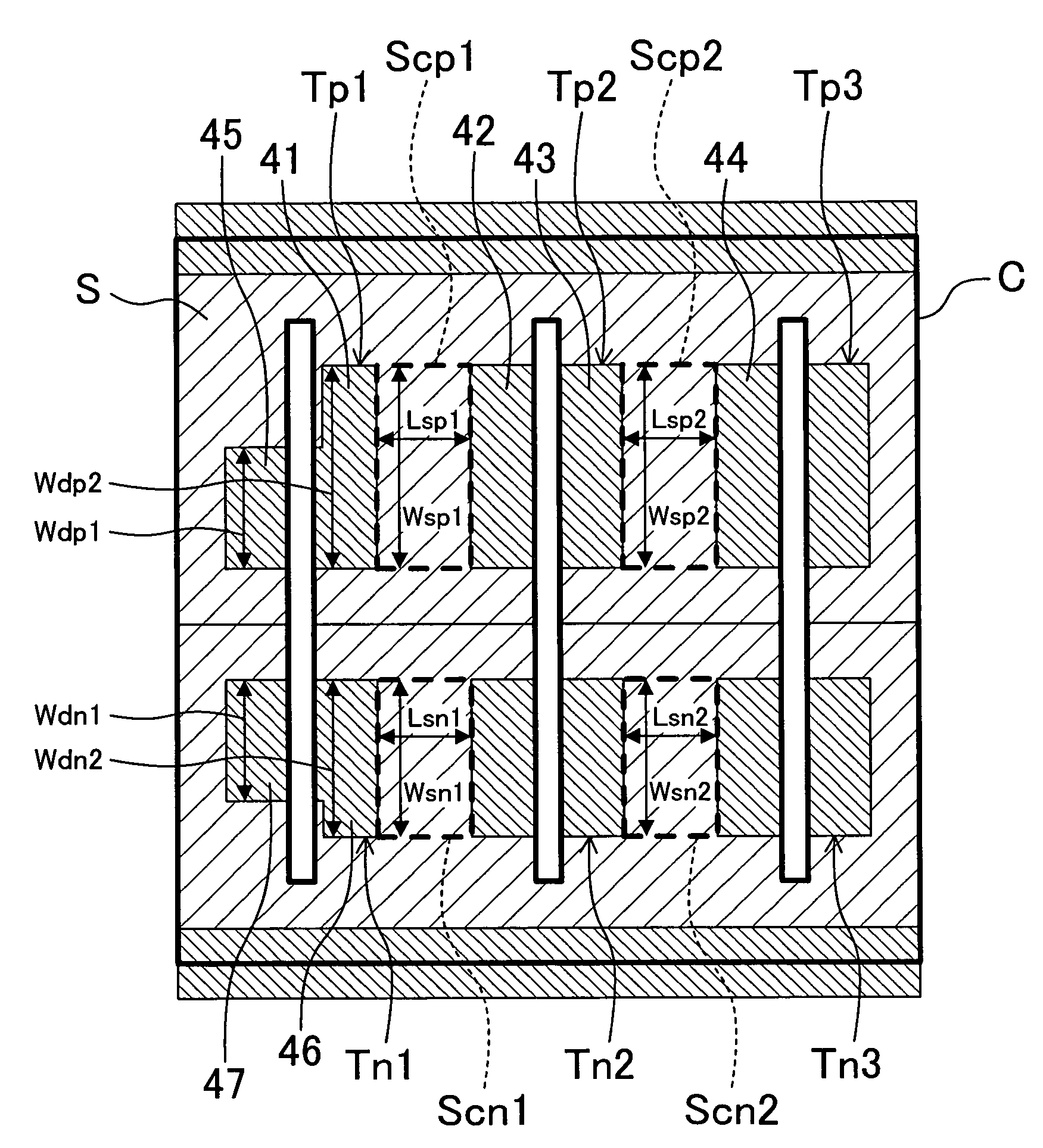
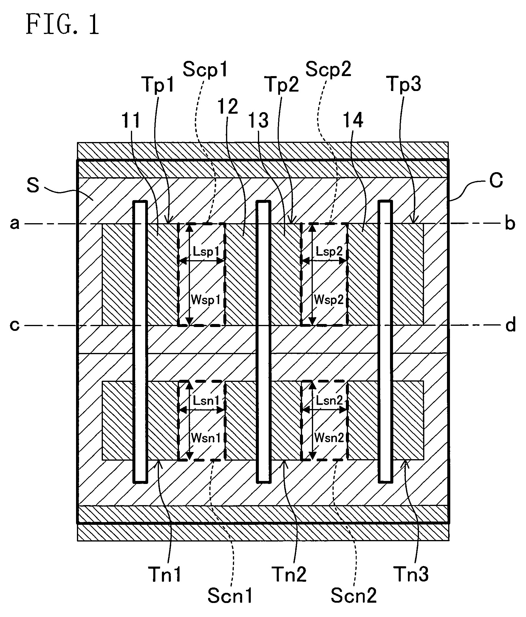
[0056]FIG. 1 is a plan view showing an example of a cell structure according to embodiment 1 of the present invention. As shown in FIG. 1, a cell C includes P-type transistors Tp1, Tp2 and Tp3, N-type transistors Tn1, Tn2 and Tn3, and a device isolation region S. The P-type transistors Tp1, Tp2 and Tp3 have an equal gate width. The N-type transistors Tn1, Tn2 and Tn3 have an equal gate width.

[0057]In FIG. 1, the P-type transistor placement region includes an impurity diffusion region 11 (first impurity diffusion region) which is a constituent of the P-type transistor Tp1 and an impurity diffusion region 12 (second impurity diffusion region) which is a constituent of the P-type transistor Tp2. The impurity diffusion regions 11 and 12 are provided side by side in the gate length direction with the device isolation region S interposed therebetween. The impurity diffusion regions 11 and 12 constitute a diffusion region pair. Also, the P-type transistor placement region includes an impur...

embodiment 2

[0067]FIG. 4 is a plan view showing an example of a cell structure according to embodiment 2 of the present invention. As shown in FIG. 4, a cell C includes P-type transistors Tp1, Tp2 and Tp3, N-type transistors Tn1, Tn2 and Tn3, and a cell C2 includes a P-type transistor Tp4 and an N-type transistor Tn4.

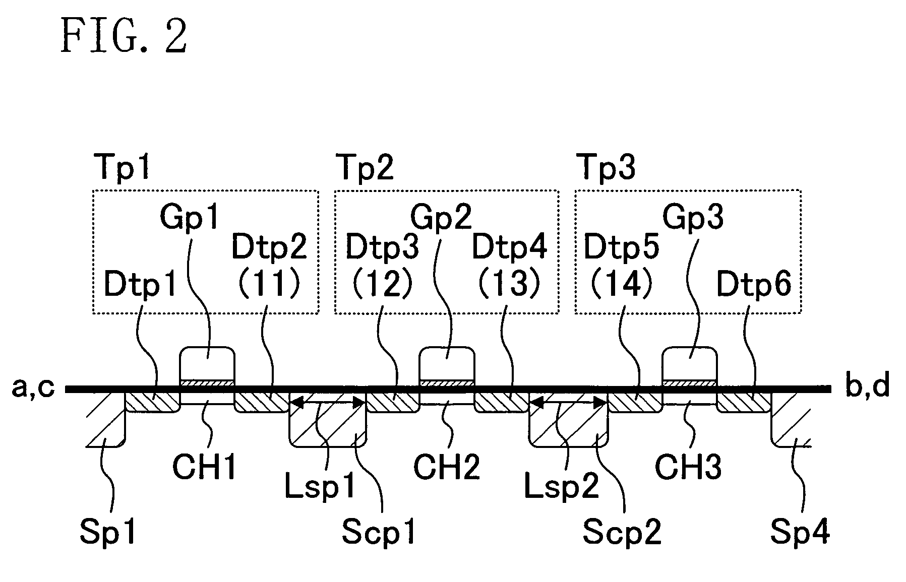
[0068]Referring to FIG. 4, in the P-type transistor placement region, part of the device isolation region S between the impurity diffusion region 11 of the P-type transistor Tp1 and the impurity diffusion region 12 of the P-type transistor Tp2 is referred to as an isolation region portion Scp1. Part of the device isolation region S between the impurity diffusion region 13 of the P-type transistor Tp2 and the impurity diffusion region 14 of the P-type transistor Tp3 is referred to as an isolation region portion Scp2. The isolation region portion Scp1 has separation length Lsp1 and separation width Wsp1, and the isolation region portion Scp2 has separation length Lsp2 and separation ...

embodiment 3

[0073]FIG. 5 is a plan view showing an example of a cell structure according to embodiment 3 of the present invention. As shown in FIG. 5, a cell C includes P-type transistors Tp1 and Tp3, N-type transistors Tn1 and Tn3, a P-type dummy impurity diffusion region Ddump, an N-type dummy impurity diffusion region Ddumn, and a device isolation region S.

[0074]In FIG. 5, the P-type transistor placement region includes an impurity diffusion region 21 (first impurity diffusion region), which is a constituent of the P-type transistor Tp1, and the dummy impurity diffusion region Ddump (second impurity diffusion region). The impurity diffusion region 21 and the dummy impurity diffusion region Ddump are provided side by side in the gate length direction with the device isolation region S interposed therebetween. The impurity diffusion region 21 and the dummy impurity diffusion region Ddump constitute a diffusion region pair. The P-type transistor placement region also includes an impurity diffus...


PUM


Abstract

A cell includes a plurality of diffusion region pairs, each of the diffusion region pairs being formed by a first impurity diffusion region which is a constituent of a transistor and a second impurity diffusion region such that the first and second impurity diffusion regions are provided side-by-side in a gate length direction with a device isolation region interposed therebetween. In each of the diffusion region pairs, the first and second impurity diffusion regions have an equal length in the gate width direction and are provided at equal positions in the gate width direction, and a first isolation region portion, which is part of the device isolation region between the first and second impurity diffusion regions, has a constant separation length. In the diffusion region pairs, the first isolation region portions have an equal separation length.

Description

CROSS-REFERENCE TO RELATED APPLICATIONS[0001]This application claims priority under 35 U.S.C. §119(a) on Japanese Patent Application No. 2006-10717 filed on Jan. 19, 2006 and Japanese Patent Application No. 2006-312705 filed on Nov. 20, 2006, the entire contents of which are hereby incorporated by reference.BACKGROUND OF THE INVENTION[0002]1. Field of the Invention[0003]The present invention relates to a semiconductor device designed by arranging a plurality of cells and specifically to a cell physical structure which enables suppression of variation in transistor characteristics in a cell.[0004]2. Description of the Related Art[0005]In recent years, in an LSI designed under a standard cell scheme, the layout pattern and arrangement of semiconductor circuit elements have been causing greater effects on the performance of the circuit along with the advancement of semiconductor process miniaturization. Therefore, high precision is required for cell circuit design, and accordingly, the...

Claims


Application Information

Patent Timeline
Patent Type & Authority Patents(United States)
IPC IPC(8): H01L21/76
CPCH01L27/0207H01L27/11898H01L27/11807
Inventor NAKANISHI, KAZUYUKI
Owner SOCIONEXT INC
Why Eureka
Try Eureka