Leadless plastic chip carrier with contact standoff

a lead-less, plastic chip technology, applied in the direction of semiconductor devices, semiconductor/solid-state device details, electrical apparatus, etc., can solve the problem of limiting the packaging density of such prior art devices, achieve better solder assembly to a pcb, facilitate solder mounting, and reduce the stress at the pcb

Active Publication Date: 2009-09-29
UTAC HEADQUARTERS PTE LTD
View PDF56 Cites 67 Cited by
  • Summary
  • Abstract
  • Description
  • Claims
  • Application Information

AI Technical Summary

Benefits of technology

[0007]Advantageously, the process provides solder bump standoff at the contact pads and die attach pad locations. This facilitates solder mounting to the printed circuit board (PCB), allowing for better solder assembly to a PCB and reduced stresses at the PCB. This is accomplished while maintaining improved package density, thermal performance and electrical performance over traditional QFP packages. Also, the solder bump standoff eases rework of packages that are soldered to a PCB.
[0008]After etching away the remainder of the leadframe strip, the contact pads and the die attach pads of each of the units of the leadframe strip are electrically isolated. However, the molding material holds the strip together in a single piece, thereby permitting electrical functional testing for each device while still in a strip.

Problems solved by technology

The inner leads terminate in outer leads that are bent down to contact a mother board, thereby limiting the packaging density of such prior art devices.

Method used


Image

  • Leadless plastic chip carrier with contact standoff
  • Leadless plastic chip carrier with contact standoff
  • Leadless plastic chip carrier with contact standoff

Examples


Embodiment Construction

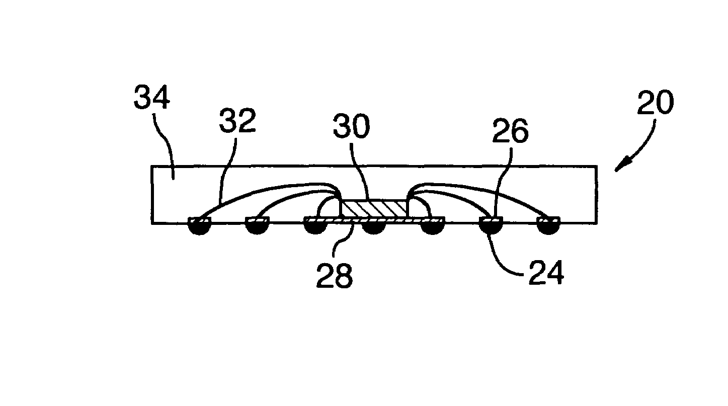
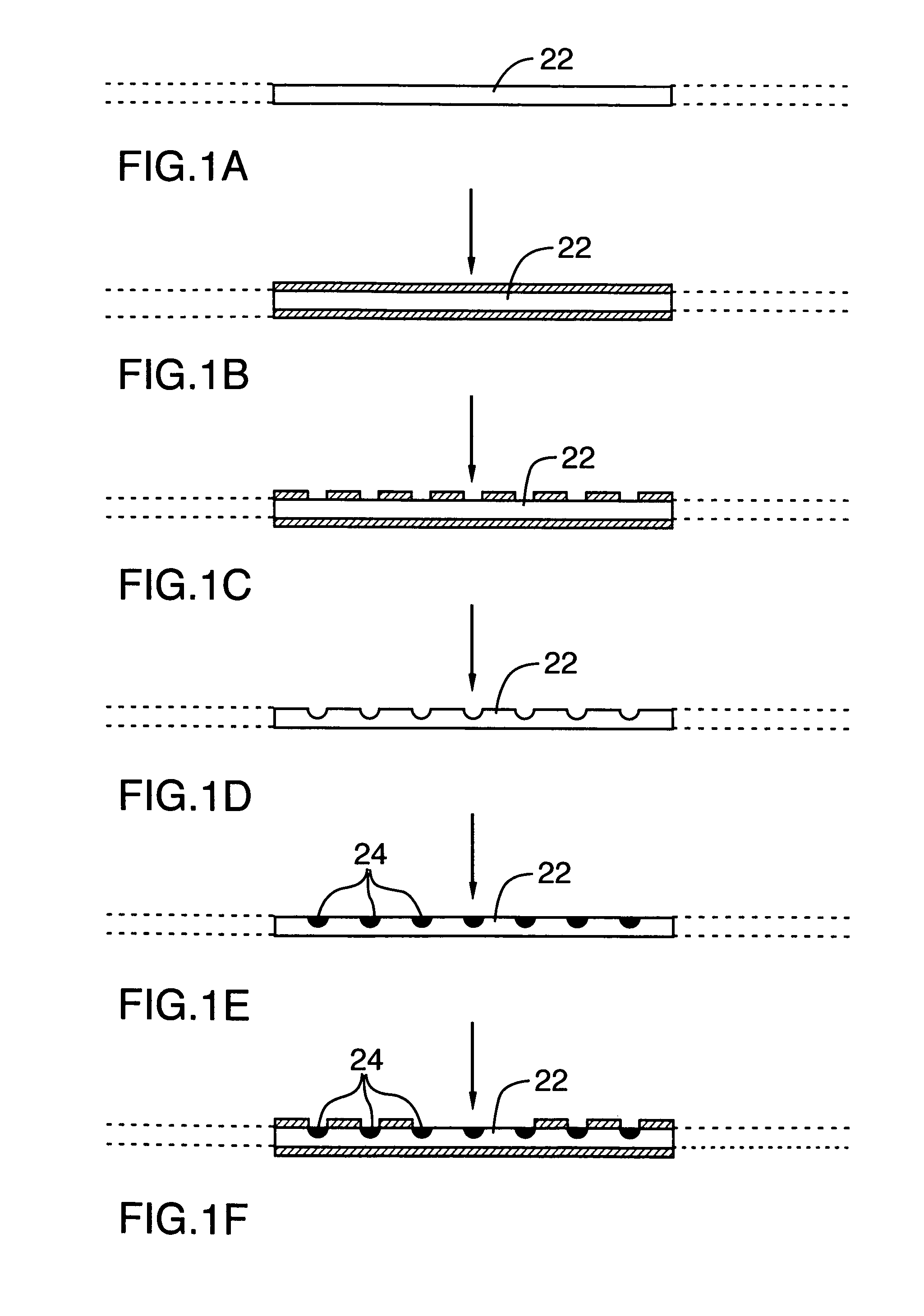
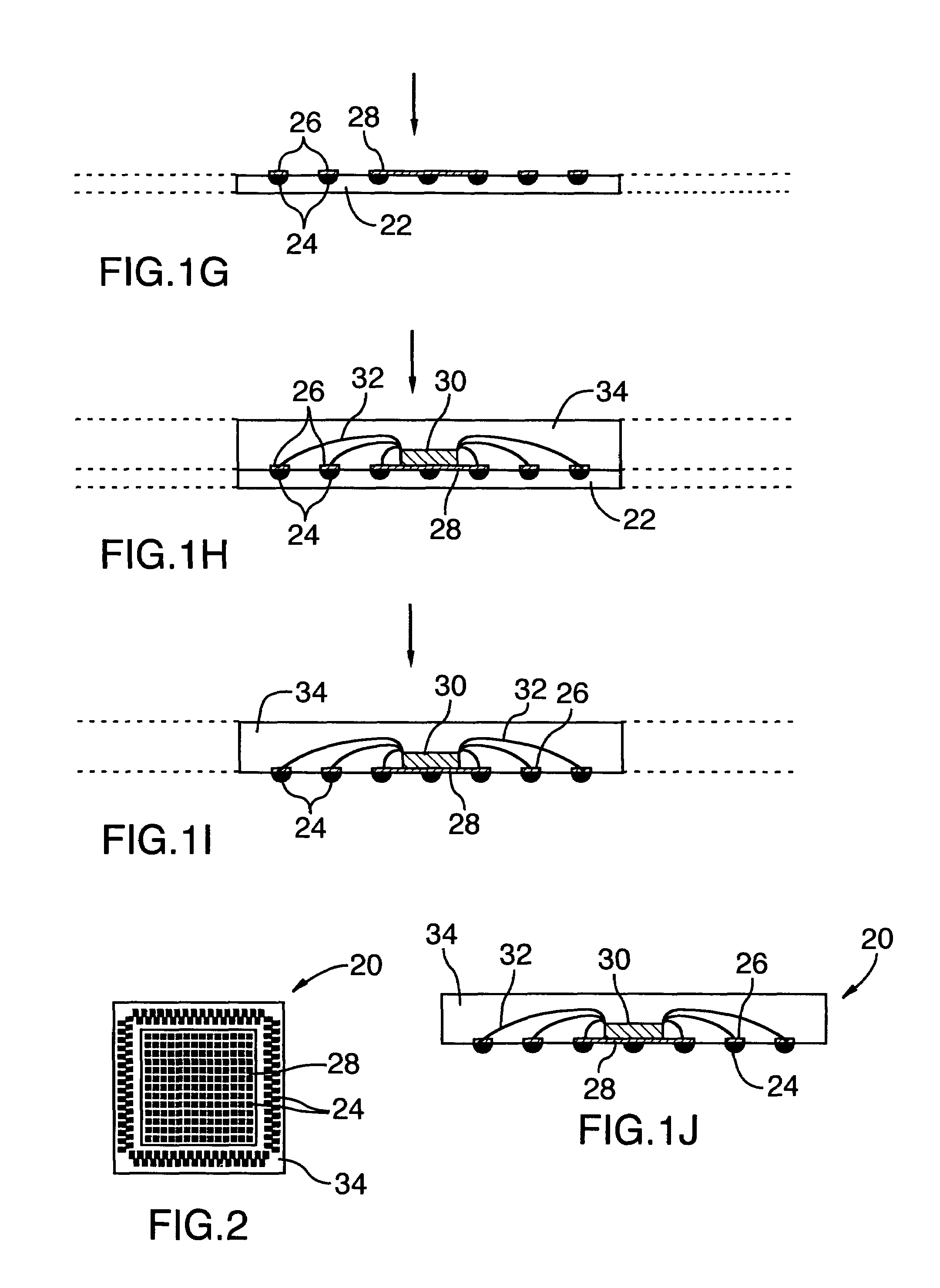
[0014]Reference is made to FIGS. 1A to 1J and FIG. 2 to describe a process for fabricating a leadless plastic chip carrier (LPCC) according to an embodiment of the present invention. The LPCC is best shown in the sectional side view of FIG. 1J and is indicated generally by the numeral 20. In fabricating the LPCC 20, a first surface of a leadframe strip 22 is selectively etched to thereby provide depressions in the first surface, and metal contacts 24 are deposited in the depressions in the first surface of the leadframe strip 22. At least one layer of metal is selectively plated on at least the metal contacts to provide a plurality of selectively plated contact pads 26 and a die attach pad 28. A semiconductor die 30 is mounted on the first surface of the die attach pad 28 and the semiconductor die 30 is wire bonded to ones of the contact pads 26. The wire bonds 32 and the semiconductor die 30 are encapsulated in a molding material 34 such that the molding material 34 covers the die ...


PUM


Abstract

A process for fabricating a leadless plastic chip carrier. A first surface of a leadframe strip is selectively etched to thereby provide depressions in the first surface and metal contacts are deposited in the depressions in the first surface of the leadframe strip. At least one layer of metal is selectively plated on at least the metal contacts to provide a plurality of selectively plated contact pads and a die attach pad. A semiconductor die is mounted on the first surface of the die attach pad and the semiconductor die is wire bonded to ones of the contact pads. The wire bonds and the semiconductor die are encapsulated in a molding material such that the molding material covers the die attach pad and the contact pads. The leadframe strip is etched away thereby exposing the metal contacts in the form of an array and the leadless plastic chip carrier is singulated from other leadless plastic chip carriers.

Description

FIELD OF THE INVENTION[0001]The present invention relates in general to integrated circuit packaging and more particularly to an improved leadless plastic chip carrier including solder bump standoff at the contact pads and die attach pad locations.BACKGROUND OF THE INVENTION[0002]According to well known prior art IC (integrated circuit) packaging methodologies, semiconductor dice are singulated and mounted using epoxy or other conventional means onto respective die pads (attach paddles) of a leadframe strip. Traditional QFP (Quad Flat Pack) packages incorporate inner leads which function as lands for wire bonding the semiconductor die bond pads. These inner leads typically require mold locking features to ensure proper positioning of the leadframe strip during subsequent molding to encapsulate the package. The inner leads terminate in outer leads that are bent down to contact a mother board, thereby limiting the packaging density of such prior art devices.[0003]In order to overcome ...

Claims


Application Information

Patent Timeline
Patent Type & Authority Patents(United States)
IPC IPC(8): H01L21/00
CPCH01L21/4832H01L23/49582H01L2924/15747H01L2924/01028H01L24/48H01L2924/15311H01L2924/01079H01L24/45H01L2224/45144H01L2224/48091H01L2224/48247H01L2224/48257H01L2224/85001H01L2924/01046H01L2924/01078H01L2924/00014H01L2924/00H01L2924/14H01L2924/181
Inventor FAN, CHUN HOKWAN, KIN PULWONG, HOI CHIMCLELLAN, NEIL
Owner UTAC HEADQUARTERS PTE LTD
Why Eureka
Try Eureka