Method and its apparatus for inspecting defects

a technology of defect inspection and defect image, which is applied in the direction of television system, semiconductor/solid-state device testing/measurement, instruments, etc., can solve the problems of difficult to accurately detect pattern images, uneven thickness of insulating film, etc., and achieve the effect of improving resolution and increasing effective na

Inactive Publication Date: 2009-10-06
HITACHI HIGH-TECH CORP
View PDF18 Cites 25 Cited by
  • Summary
  • Abstract
  • Description
  • Claims
  • Application Information

AI Technical Summary

Benefits of technology

[0008]In one aspect, the present invention is a defect inspection method and defect inspection apparatus solving the above subjects, increasing effective NA for improved resolution, and thus allowing optical inspection and observation of defects down to substantially a sub-100 nm level or below.
[0009]In another aspect, the present invention is a defect inspection method and defect inspection apparatus allowing high-sensitivity inspection by minimizing any effects of the unevenness of transparent films in film thickness when comparative inspections with adjacent dies or the like are to be conducted.
[0010]An object of the present invention is to improve the resolution of a detection optical system by filling the clearance between its objective lens and the above-mentioned sample, with a liquid, and increasing effective NA (numerical aperture).

Problems solved by technology

In the generation of hyperfine-structuring into pattern sizes of sub-100 nm, however, pattern images have been becoming difficult to accurately detect, since sufficient resolution has not been made obtainable using only the resolution-improved defect inspection optical system mentioned above.
This insulating film has thickness unevenness in the wafer.
During observation through a dry-system lens, however, thin-film interference on the transparent film causes the unevenness of the film thickness to appear as the unevenness of brightness on the image detected.
For example, during comparative inspection with respect to adjacent dies, if the transparent films on these adjacent dies are uneven in film thickness, differences in the brightness of the respective images detected will occur and an image of the object will be incorrect-detected as a defect image.
Increasing an inspection threshold value in an attempt to avoid such incorrect-detection will pose the problem that total inspection sensitivity decreases.

Method used


Image

  • Method and its apparatus for inspecting defects
  • Method and its apparatus for inspecting defects
  • Method and its apparatus for inspecting defects

Examples


Embodiment Construction

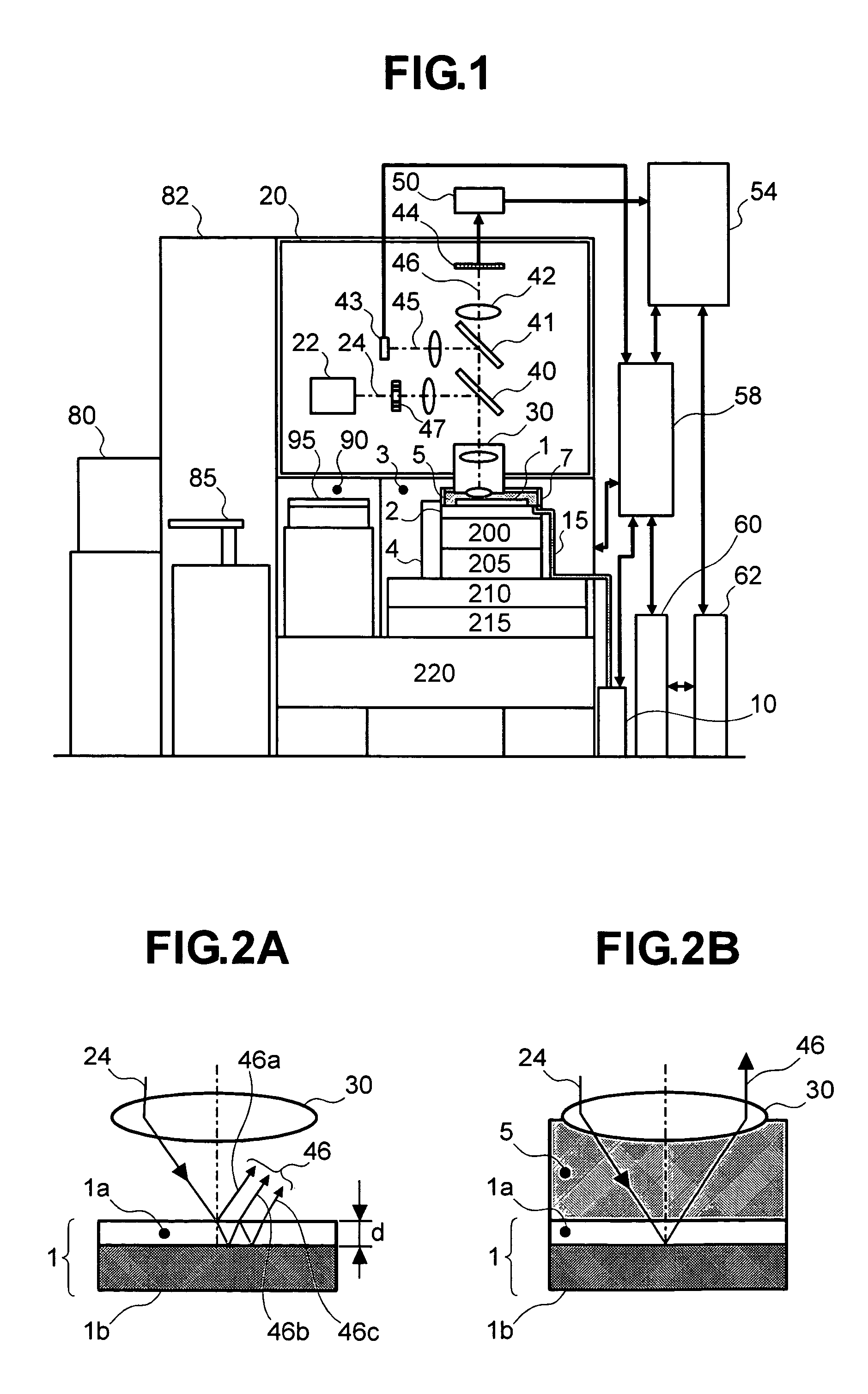
[0059]Embodiments of the present invention are described below using the accompanying drawings.

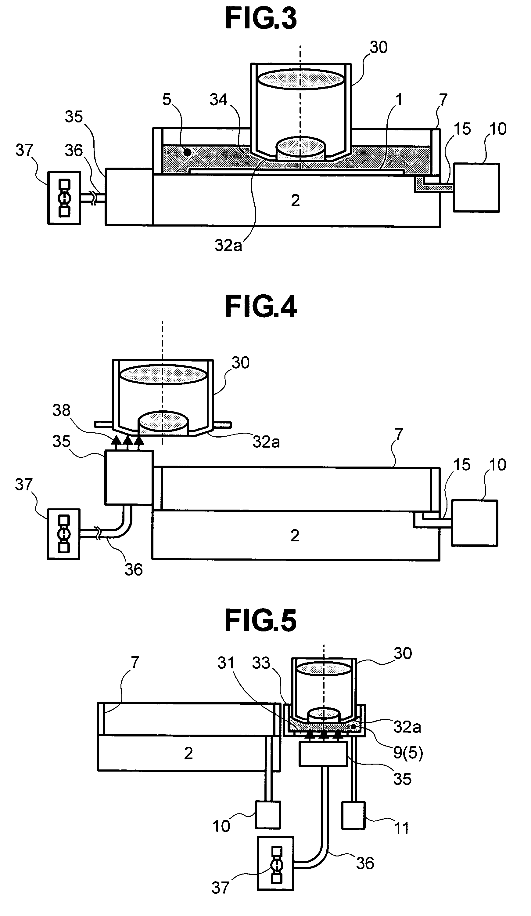
[0060]First, embodiments of the inspection that uses total liquid immersion are described using FIGS. 1 to 10, 26, 31, and 32.

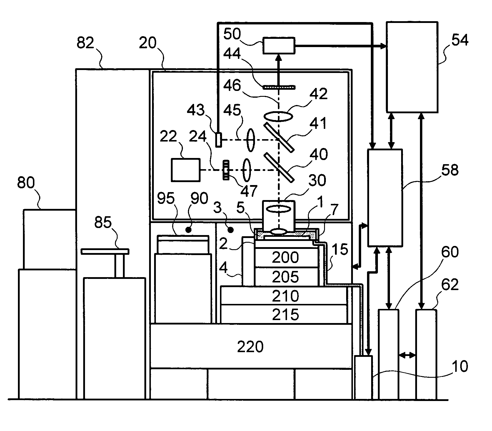
[0061]An embodiment in which the present invention is applied to an optical-type visual inspection apparatus for semiconductor wafers is shown in FIG. 1. An inspection sequence and related methods are shown in FIG. 26. Referring back to FIG. 1, symbol 82 denotes an outer frame including a wafer transfer robot 85 in an optical-type visual inspection apparatus. Wafers to be inspected are stored in a cassette 80, and each of the wafers is transferred to an inspection preparation chamber 90 by a transfer system such as the wafer transfer robot 85 (step S262, FIG. 26), and then mounted on a wafer notch (or orientation flat) detector 90. On the notch detector 90, the wafer is pre-aligned in a required a direction (step S263). After this, the wafer undergoes pre-inspection...


PUM

PropertyMeasurementUnit
refractive indexaaaaaaaaaa

Abstract

The present invention relates to a high-sensitivity inspection method and apparatus adapted for the fine-structuring of patterns, wherein defect inspection sensitivity is improved using the following technologies: detection optical system is improved in resolution by filling the clearance between an objective lens 30 and a sample 1, with a liquid, and increasing effective NA (Numerical Aperture); and when a transparent interlayer-insulating film is formed on the surface of the sample, amplitude splitting at the interface between the liquid and the insulating film is suppressed for reduction in the unevenness of optical images in brightness due to interference of thin-film, by immersing the clearance between the objective lens and the sample, with a liquid of a refractive index close to that of the transparent film.

Description

BACKGROUND OF THE INVENTION[0001]The present invention relates to a defect inspection method and defect inspection apparatus used to inspect and observe defects, foreign particle, and the like, on the micro-patterns formed on a substrate through a thin-film forming process represented by manufacturing processes for semiconductors or flat-panel displays.[0002]Fine structuring of the patterns formed with photolithography is progressing with the enhancement of semiconductor integration density and the improvement of flat-panel display resolution. During the manufacturing processes for these products, after the patterns have been formed, they are subjected to defect inspection and / or the like in order to improve production yields. During the defect inspection, the patterns are detected as images by optical system etc., then these images are compared with those of adjacent dies (or cells), and defects are extracted on the basis of comparison results.[0003]Incidentally, the resolution-imp...

Claims


Application Information

Patent Timeline
Patent Type & Authority Patents(United States)
IPC IPC(8): G06K9/00H04N7/18G01B11/30G01N21/13G01N21/15G01N21/88G01N21/95G01N21/956H01L21/66
CPCG01N21/8806G01N21/9501G01N21/95623G01N21/95607G01N21/13G01N2021/9513G01N2021/154G01N2021/8825
Inventor SHIBATA, YUKIHIROMAEDA, SHUNJIKUBOTA, HITOSHI
Owner HITACHI HIGH-TECH CORP
Why Eureka
Try Eureka