Method and apparatus for inspecting defects and a system for inspecting defects

a technology of defect inspection and defect, applied in semiconductor/solid-state device testing/measurement, instruments, material analysis, etc., can solve the problems of increasing apparatus costs, affecting the accuracy of inspection, and reducing the effectiveness of inspection, so as to improve the effective na and improve the resolution

Inactive Publication Date: 2008-05-13
HITACHI HIGH-TECH CORP
View PDF6 Cites 14 Cited by
  • Summary
  • Abstract
  • Description
  • Claims
  • Application Information

AI Technical Summary

Benefits of technology

[0006]In order to solve the above problems, the present invention relates to a defect inspection method, defect inspection apparatus, and defect inspection system which enables defects that are ultrafine than patterns of about sub-100-nm or less to be optically inspected and observed by increasing effective NA for improved resolution.
[0007]In one aspect, the present invention is a defect inspection method for detecting with an image sensor the optical image of a sample that has been enlarged and projected by an optical system, and thus detecting defects present on the sample; wherein an object of the present invention is to improve the optical system in resolution by filling the interspace between an objective lens and the sample with a liquid, and increasing effective NA (numerical aperture).
[0008]In another aspect, the present invention is constructed so that even when a transparent interlayer-insulating film is formed on the surface of a sample, the unevenness of brightness due to thin-film interference can be reduced since immersion of the interspace between an objective lens and the sample, in a liquid of a refractive index (ideally, 1.3 to 1.7) close to that of the interlayer-insulating film, suppresses amplitude splitting at the interface between the liquid and the insulating film.

Problems solved by technology

When it comes to the generation of sub-100 nm in terms of pattern size, however, optical systems lack resolution and pattern images become difficult to accurately detect.
However, the exposure with F2 laser light, presents problems such as increases in apparatus costs because the construction of an optical system becomes complex and decreases in exposure margins due to decreases in the depth of focus during exposure.
This insulating film has thickness unevenness in the wafer.
During observation through a dry-system lens, however, thin-film interference on the transparent film causes the unevenness of the film thickness to appear as the unevenness of brightness on the image detected.
For example, during comparative inspection with respect to adjacent dies, if the transparent films on these adjacent dies are uneven in film thickness, differences in the brightness of the respective images detected will occur and an image of the object will be incorrectly detected as a defect image.
Increasing an inspection threshold value in an attempt to avoid such incorrect detection will pose the problem that total inspection sensitivity decreases.
Also, etched patterns are usually subjected to defect inspection.

Method used


Image

  • Method and apparatus for inspecting defects and a system for inspecting defects
  • Method and apparatus for inspecting defects and a system for inspecting defects
  • Method and apparatus for inspecting defects and a system for inspecting defects

Examples


first embodiment

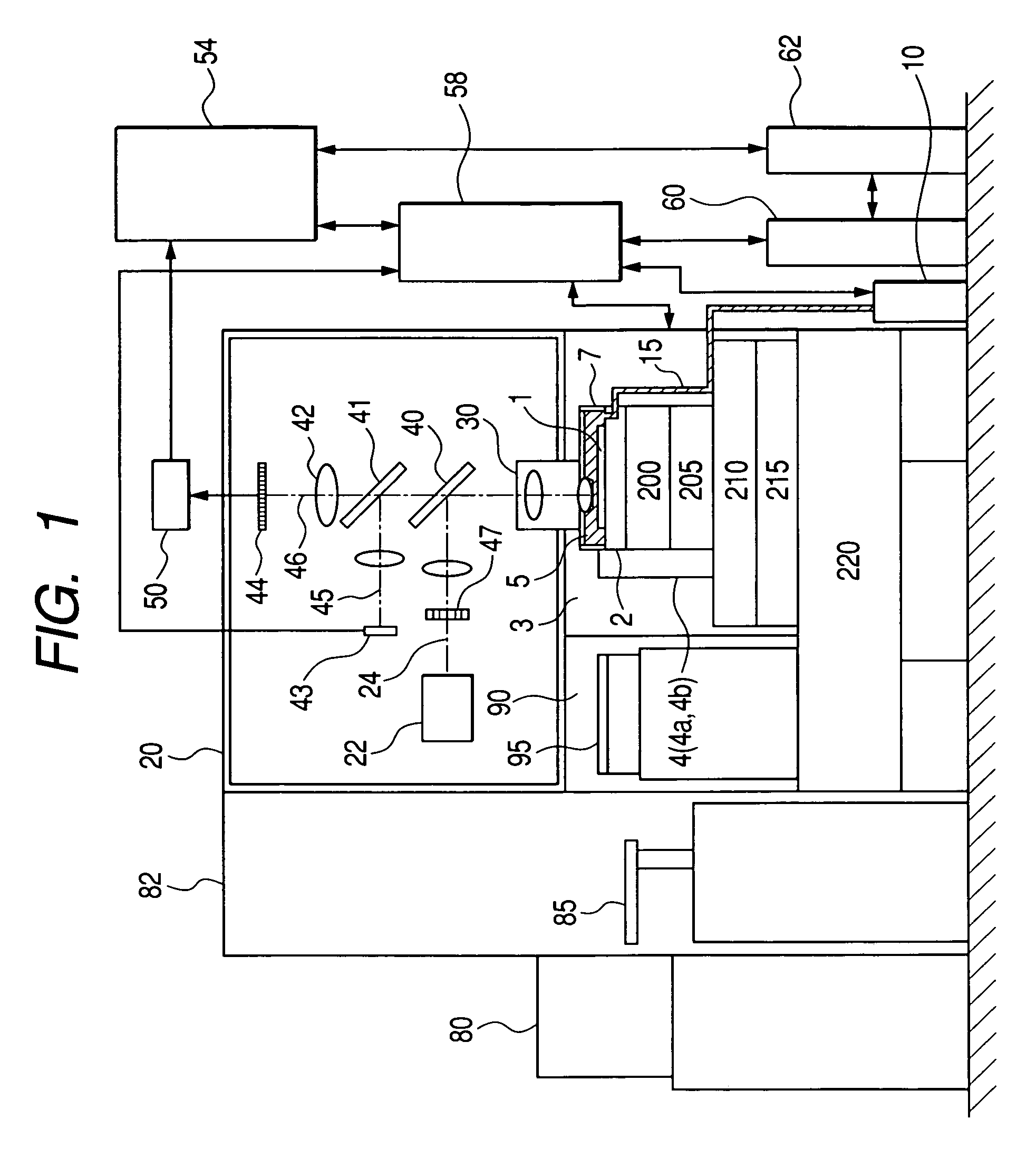
[0040]A first embodiment in which the total liquid immersion method that forms part of the liquid immersion technology according to the present invention is applied to an optical-type visual inspection apparatus for semiconductor wafers will be described using FIG. 1. Wafers to be inspected are stored in a cassette 80, and each of the wafers is transferred to an inspection preparation chamber 90 by a wafer transfer robot 85 and then mounted on a wafer notch (or orientation flat) detector unit 95. The wafer is prealigned in a desired direction by the wafer notch detector unit 95. Next, the wafer is transferred to an inspection station 3. In the inspection station 3, wafer 1 is fixed by a chuck 2, and the wafer 1 is totally immersed in a liquid 5 with which a liquid tank (a liquid vessel) 7 is filled. The liquid tank 7 is connected to a liquid supply / discharge unit 10 by a pipe 15, and the liquid tank 7 supplies the liquid 5 after loading of the wafer 1, and discharges the liquid 5 be...

second embodiment

[0077]A second embodiment in which the local liquid immersion method that forms part of the liquid immersion technology according to the present invention is applied to an optical-type visual inspection apparatus for semiconductor wafers will be described using FIG. 8. Unlike the total liquid immersion method shown in FIG. 1, the local liquid immersion method is used to immerse only the interspace between the objective lens 30 and the wafer 1, in a liquid. A basic configuration of the second embodiment is much the same as that of the first embodiment, except for the inside of the inspection station 3. For example, for a linear type of image sensor 44, images are acquired while the wafer 1 is being moved at a fixed speed. A liquid 5 is fed from a liquid supply / discharge unit 10 into a liquid supply controller 181 at a specific pressure. The liquid, after having its flow rate, temperature, and other factors controlled by the liquid supply controller 181, is supplied to the surface of ...

third embodiment

[0094]Next, an example of configuration of a visual inspection optical system which uses liquid immersion, and a method for improving this optical system in resolution will be described below using FIG. 16.

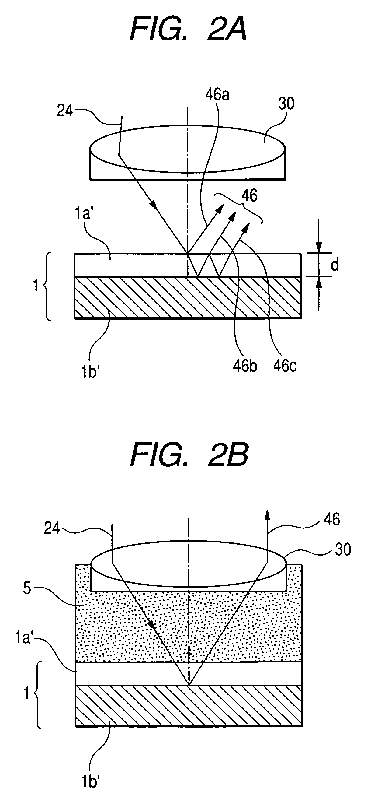
[0095](1) An interspace between an objective lens 30 and a wafer 1 is immersed in a liquid 5 and thus, resolution is improved.

[0096](2) In an incident illumination / bright-field detection scheme, when Koheler illumination is applied, an image of a light source 22 is formed on an aperture stop (an aperture diaphragm) 425. This image is further formed on a pupil of the objective lens 30. If the aperture stop 425 has a ring-form (zonal) aperture portion, light that illuminates one point on the wafer 1 becomes oblique illumination light not having a vertical illumination light component. Use of the illumination light improves high-frequency MTF (Modulation Transfer Function) of a spatial frequency.

[0097](3) Furthermore, when a polarizing type of beam splitter 40a is used, the light ref...


PUM

PropertyMeasurementUnit
wavelengthaaaaaaaaaa
refractive indexaaaaaaaaaa

Abstract

The present invention relates to a high-sensitivity defect inspection method, apparatus, and system adapted for the fine-structuring of patterns; wherein, in addition to a cleaning tank which chemically cleans a sample and rinses the sample, a defect inspection apparatus having a liquid-immersion element by which the interspace between the sample and the objective lens of an optical system is filled with a liquid, and a drying tank which dries the sample, the invention uses liquid-immersion transfer means from said cleaning tank through said liquid-immersion means of said defect inspection apparatus to said drying tank so that the sample is transferred in a liquid-immersed state from said cleaning tank to said liquid-immersion means.

Description

BACKGROUND OF THE INVENTION[0001]The present invention relates to a defect inspection method, defect inspection apparatus, and defect inspection system used to inspect and observe defects, foreign particles, and the like, on the micropatterns formed on substrates through a thin-film forming process represented by manufacturing processes for semiconductors and / or flat-panel displays.[0002]Fine-structuring of the patterns formed with photolithography is progressing with the enhancement of semiconductor integration density and the improvement of flat-panel display resolution. During the manufacturing processes for these products, the formation of the patterns is followed by defect inspection and / or the like in order to improve production yields. During the defect inspection, the patterns are detected as images by an optical system and then defects are extracted by comparing these images with those of adjacent dies (or cells). When it comes to the generation of sub-100 nm in terms of pa...

Claims


Application Information

Patent Timeline
Patent Type & Authority Patents(United States)
IPC IPC(8): G01N21/00G01N21/88G01N21/956H01L21/00H01L21/66
CPCG01N21/95607H01L21/67028H01L21/67057H01L21/67253G01N2021/4792
Inventor SHIBATA, YUKIHIROMAEDA, SHUNJIOKABE, TAKAFUMITAKAHARA, YOICHI
Owner HITACHI HIGH-TECH CORP
Why Eureka
Try Eureka