Liquid crystal display device having rectangular-shaped pixel electrodes overlapping with comb-shaped counter electrodes in plan view

a liquid crystal display and counter electrode technology, applied in non-linear optics, instruments, optics, etc., can solve the problem of limited numerical aperture enhancement, achieve the effect of eliminating display defects, increasing display brightness, and enhancing numerical apertur

Active Publication Date: 2009-10-20
PANASONIC LIQUID CRYSTAL DISPLAY CO LTD +1
View PDF8 Cites 48 Cited by
  • Summary
  • Abstract
  • Description
  • Claims
  • Application Information

AI Technical Summary

Benefits of technology

[0011]It is an object of the present invention to provide a lateral-electric-field-type liquid crystal display device which can enhance a numerical aperture of pixels thus realizing a bright image display.
[0027]According to the constitution of the present invention, the thin film transistor and the contact hole portion which connects an output electrode of the TFT to the pixel electrode which have been considered as portions which do not contribute to a display in the pixel region can be used as the reflective display region and hence, it is possible to enhance a numerical aperture and to increase a display brightness. Further, conventionally, thicknesses of the electrode and the insulation film which have been formed on the contact hole portion are reduced compared to thicknesses of the electrode and the insulation film which have been formed on a leveled surface portion and hence, there exists a possibility that short-circuiting occurs between the counter electrode and the pixel electrode which are formed on the contact hole portion. According to the present invention which eliminates the mounting of the counter electrode on the contact hole portion, it is possible to avoid the occurrence of the above-mentioned short-circuiting.
[0028]Further, according to the present invention, since the surface of the insulation film can be leveled by embedding the insulation member in the opening formed in the insulation film which is formed on the contact hole portion, the orientation film which is formed over the insulation film can be leveled. Accordingly, it is also possible to impart the accurate orientation to the liquid crystal on the contact hole portion in the same manner as other portions thus eliminating a display defect such as a light leakage or the like attributed to the defective orientation.

Problems solved by technology

Accordingly, the increase of an effective area of the pixel, that is, the enhancement of a numerical aperture is limited.

Method used


Image

  • Liquid crystal display device having rectangular-shaped pixel electrodes overlapping with comb-shaped counter electrodes in plan view
  • Liquid crystal display device having rectangular-shaped pixel electrodes overlapping with comb-shaped counter electrodes in plan view
  • Liquid crystal display device having rectangular-shaped pixel electrodes overlapping with comb-shaped counter electrodes in plan view

Examples


embodiment 1

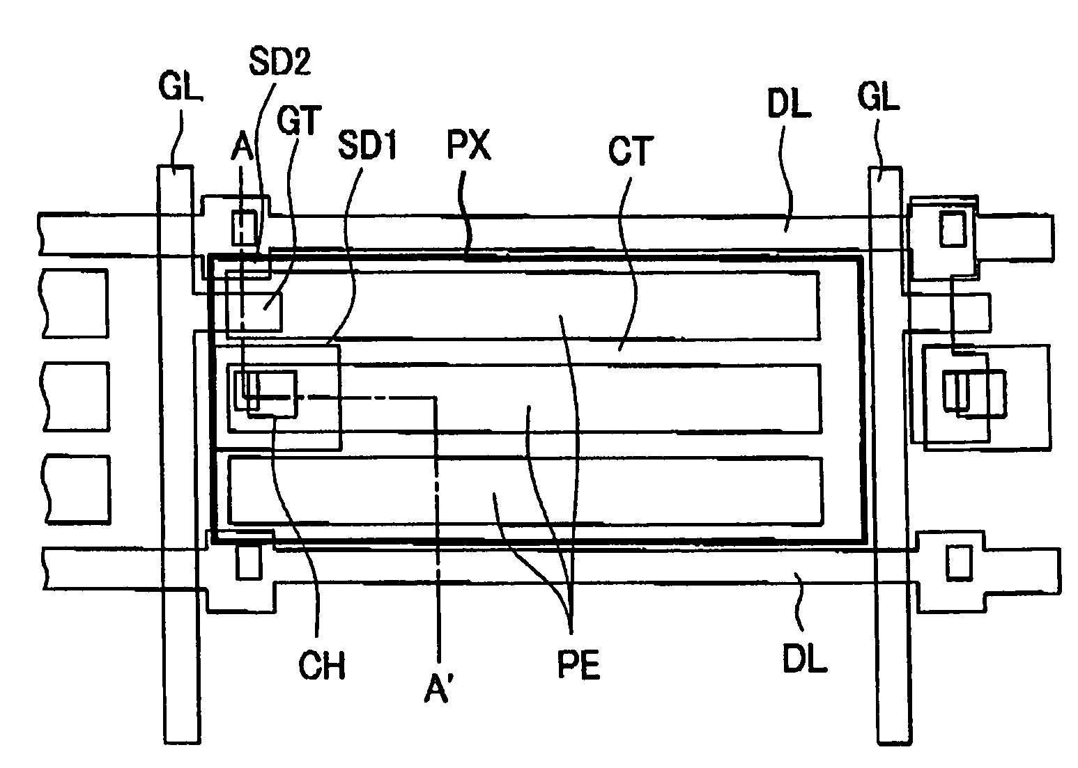
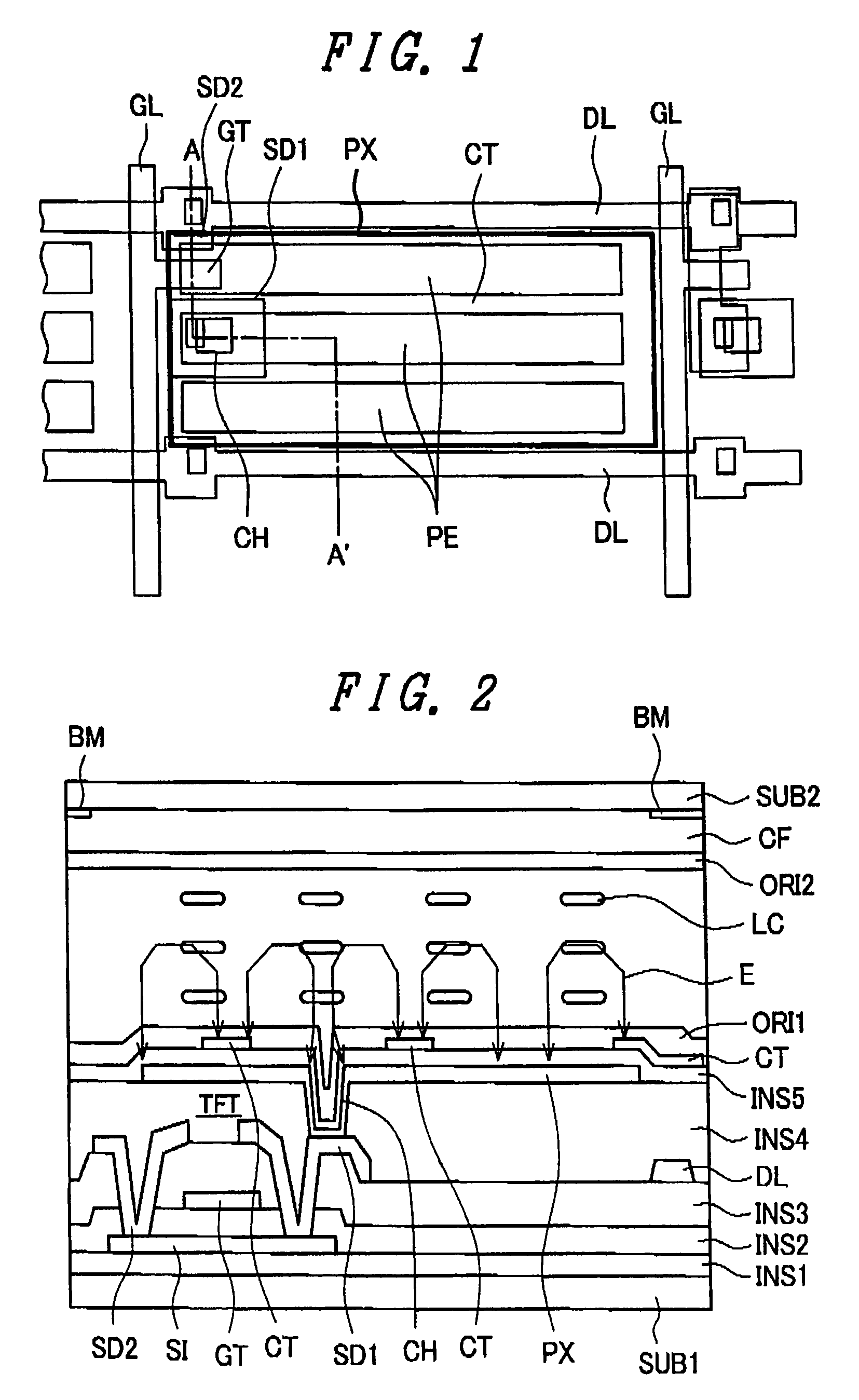
[0040]FIG. 1 is a plan view which shows an example of the constitution of one pixel for explaining an embodiment 1 of a liquid crystal display device according to the present invention. Further, FIG. 2 is a cross-sectional view taken along a line A-A′ in FIG. 1. This liquid crystal display device is of an IPS type. In the same manner as the display device shown in FIG. 10, a pixel region is formed in a region which is surrounded by two scanning lines (hereinafter, also referred to as gate lines) GL and two image signal lines (hereinafter, also referred to as data lines) DL. A thin film transistor TFT which constitutes an active element is formed in a portion of the pixel region. The thin film transistor TFT has a drain (or a source) electrode SD2 thereof connected to the data line DL, has a gate electrode GT thereof connected to the gate line GL and has a source (a drain) electrode SD1 thereof connected to a pixel electrode PX via a contact hole CH.

[0041]As shown in FIG. 2 which is ...

embodiment 2

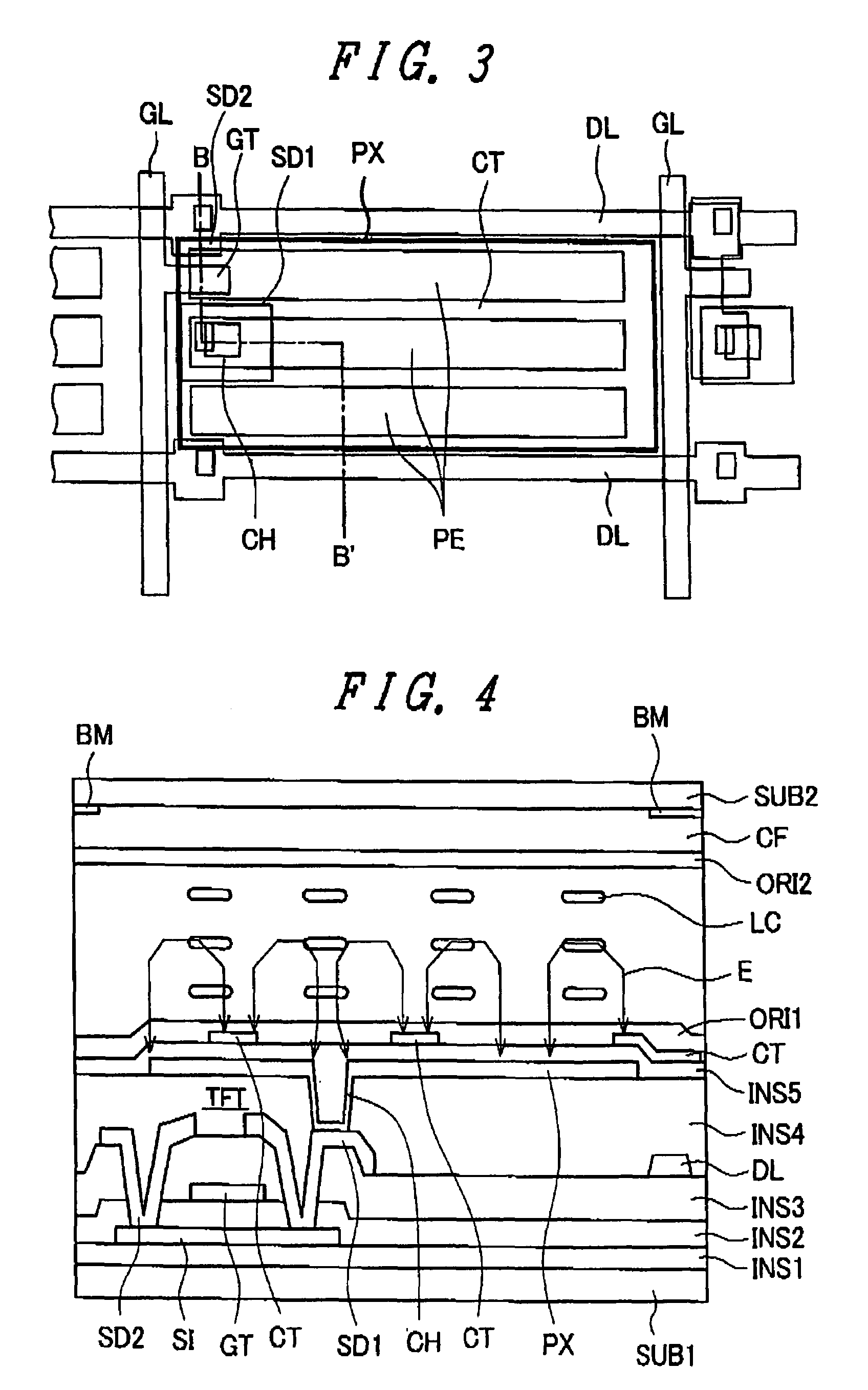
[0056]FIG. 3 is a plan view which shows an example of the constitution of one pixel for explaining an embodiment 2 of a liquid crystal display device according to the present invention, while FIG. 4 is a cross-sectional view taken along a line B-B′ in FIG. 3. The liquid crystal display device of the embodiment 2 is also of an IPS type. In the same manner as the embodiment 1, a pixel region is formed in the inside of a region which is surrounded by two gate lines GL and two data lines DL. A thin film transistor TFT is formed at a portion of the pixel region. The thin film transistor TFT has a drain (or a source) electrode SD2 thereof connected to the data line DL, has a gate electrode GT thereof connected to the gate line GL, and has a source (a drain) electrode SD1 thereof connected to a pixel electrode PX via a contact hole CH.

[0057]As shown in FIG. 4 which is a cross-sectional view taken along a line B-B′ in FIG. 3, the cross-sectional structure of the pixel includes the thin film...

embodiment 3

[0064]FIG. 5 is a plan view which shows an example of the structure of one pixel for explaining an embodiment 3 of the liquid crystal display device according to the present invention, while FIG. 6 is a cross-sectional view taken along a line C-C′ in FIG. 5. The liquid crystal display device of the embodiment 3 is also of an IPS type. In the same manner as the embodiment 1 and the embodiment 2, a pixel region is formed in the inside of a region which is surrounded by two gate lines GL and two data lines DL. A thin film transistor TFT is formed at a portion of the pixel region. The thin film transistor TFT has a drain (or a source) electrode SD2 thereof connected to the data lines DL, has a gate electrode GT thereof connected to the gate lines GL and has a source (a drain) electrode SD1 there of connected to a pixel electrode PX via a contact hole CH.

[0065]As shown in FIG. 6 which is a cross-sectional view taken along a line C-C′ in FIG. 5, the cross-sectional structure of the pixel ...


PUM

PropertyMeasurementUnit
thicknessaaaaaaaaaa
thicknessaaaaaaaaaa
thicknessaaaaaaaaaa

Abstract

The present invention realizes a bright image display by enhancing a numerical aperture of pixels. At least a portion of a pixel electrode is overlapped to a thin film transistor by way of a first insulation film, the pixel electrode is connected to an output electrode of the thin film transistor via a contact hole which is formed in the first insulation film, the counter electrode is arranged above the pixel electrode by way of a second insulation film in a state that the counter electrode is overlapped to the pixel electrode, the counter electrode is formed at a position avoiding the contact hole formed in the first insulation film as viewed in a plan view, and at least a portion of the counter electrode is overlapped to the thin film transistor.

Description

[0001]The present application claims priority from Japanese application JP2005-278161 filed on Sep. 26, 2005, the content of which is hereby incorporated by reference into this application.BACKGROUND OF THE INVENTION[0002]The present invention relates to a liquid crystal display device, and more particularly to a lateral-electric-field-type liquid crystal display device which can enhance a display numerical aperture.[0003]As a display device for various kinds of personal digital assistants and television receiver sets, a display device which uses a so-called flat-type display panel as represented by a liquid crystal display device has been a mainstream. Further, as the liquid crystal display device, an active-method-type liquid crystal display device has been popularly used. The active-method-type liquid crystal display device generally uses a thin film transistor as a drive element of a pixel and hence, hereinafter, the display device which adopts the thin film transistor as the dr...

Claims


Application Information

Patent Timeline
Patent Type & Authority Patents(United States)
IPC IPC(8): G02F1/1343
CPCG02F1/136G02F1/136227G02F1/133345G02F2201/40G02F1/133305G02F1/134363G02F1/136277G02F1/1368
Inventor OCHIAI, TAKAHIROSASAKI, TOHRUIMAYAMA, HIROTAKAMORIMOTO, MASATERU
Owner PANASONIC LIQUID CRYSTAL DISPLAY CO LTD
Why Eureka
Try Eureka