
Switch circuit of an image sensor for changing resolution and a method thereof

a technology of image sensor and switch circuit, which is applied in the direction of television system, pulse technique, instruments, etc., can solve the problems of high production cost, complex wiring structure, and large noise in the circuit, so as to reduce the cost of the circuit, avoid any negative effects of noise, and increase the signal/noise ratio

Active Publication Date: 2009-10-27
DYNA IMAGE CORPORATION
View PDF4 Cites 0 Cited by
  • Summary
  • Abstract
  • Description
  • Claims
  • Application Information

AI Technical Summary

Benefits of technology

"The present invention provides a resolution switch circuit for an image sensor that avoids the need for additional resolution switch circuits, reducing noise and improving signal-to-noise ratio. The circuit uses a switch capacitor to transmit image signals, preventing signal distortion and increasing signal uniformity. It also eliminates the need for transistors used in conventional optical signal converting units, reducing production costs. The circuit allows for changing resolution values and includes a control unit to manage image gathering units and a resolution control unit to control shift registers. The invention provides a method for changing resolution values for an image sensor by controlling image gathering units, shift registers, and a signal combining unit. Overall, the invention improves image quality and reduces costs."

Problems solved by technology

Such a switch circuit produces a lot of noise, and thus suffers from signal uniformity, high production costs and a complex wiring structure.

Method used


Image

  • Switch circuit of an image sensor for changing resolution and a method thereof
  • Switch circuit of an image sensor for changing resolution and a method thereof
  • Switch circuit of an image sensor for changing resolution and a method thereof

Examples


first embodiment

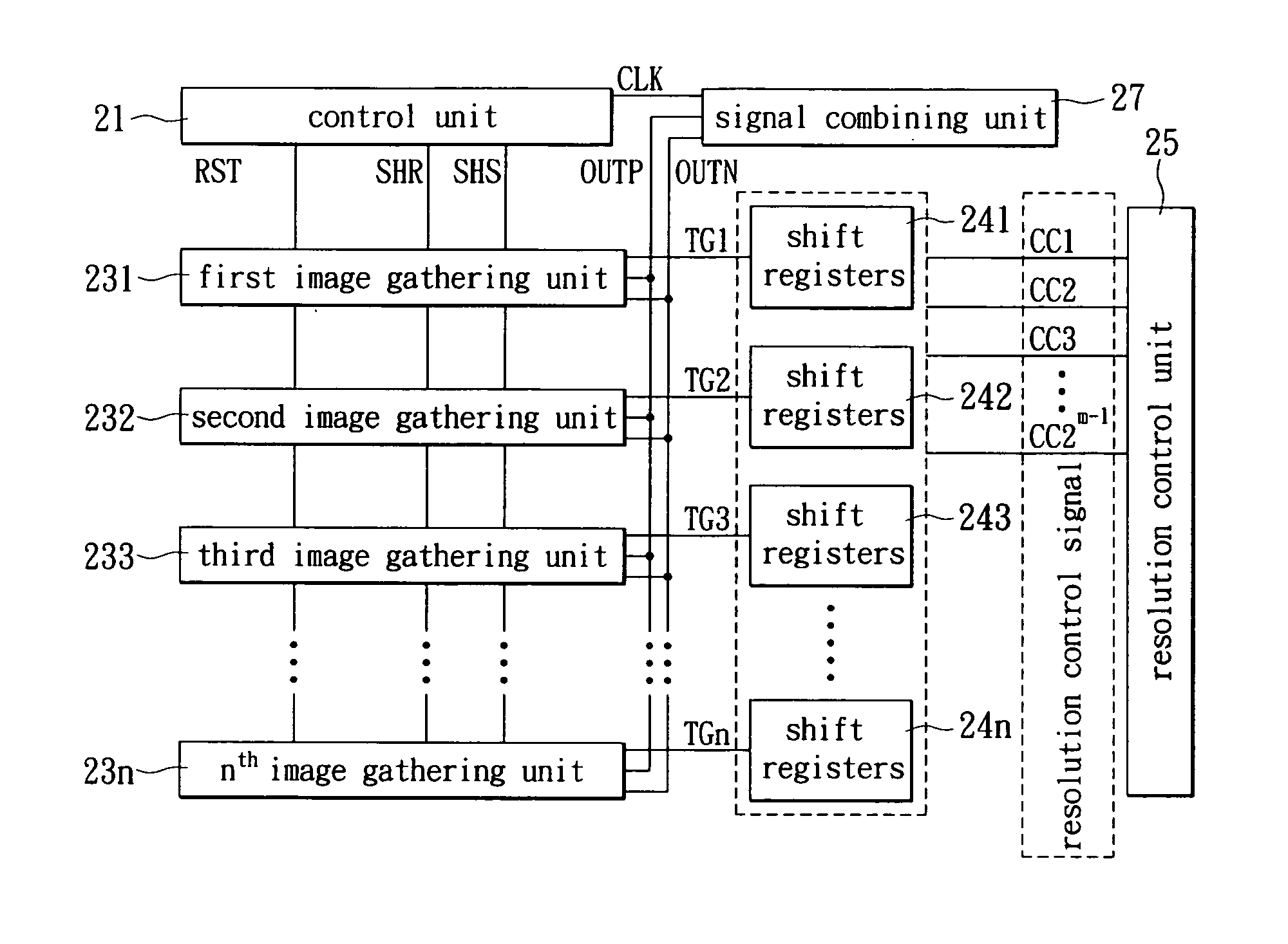
[0025]In the signal combing unit 27, the fourth control signal CLK from the control unit 21 and the first image signal and the second image signal from the image gathering units 231-23n are combined. FIG. 4A is a circuit diagram showing a signal combining unit according to the invention. The signal combining unit 27A includes a double-input / output operational amplifier O27, a sixth switch S6, a seventh switch S7, a capacitor C271, and a capacitor C272. The sixth switch S6 connects to the capacitor C271 in series, and further connects to the first signal receiving terminal IN1 and a first output terminal OT1 of the operational amplifier O27. The seventh switch S7 connects to the capacitor C272 in series, and further connects to a second signal receiving terminal IN2 and a second output terminal OT2 of the operational amplifier O 27. The first signal receiving terminal IN1 connects to the first image output wiring OUTP to receive the first image signal. The second output terminal OT2 ...

second embodiment

[0026]FIG. 4B is a circuit diagram of a signal combining unit according to the invention. The signal combining unit 27B includes a first operational amplifier O271, a second operational amplifier O272, a eighth switch S8, a ninth switch S9, a capacitor C273, and a capacitor C274. The eighth switch S8 connects to the capacitor C273 in series, and further connects to the first signal receiving terminal IN 71 and the first output terminal OT71 of the first operational amplifier O271. The ninth switch S9 connects to the capacitor C274 in series and further connects to the second signal receiving terminal IN72 and the second output terminal OT72 of the second operation amplifier O272. The first signal receiving terminal IN71 connects to the first image output wiring OUTP to receive the first image signal. The second output terminal OT72 connects to the second image output wiring OUTN to receive the second image signal. The first other terminals of the first operational amplifier O271 and...


PUM

PropertyMeasurementUnit
transmissionaaaaaaaaaa
weightaaaaaaaaaa
signal/noise ratioaaaaaaaaaa

Abstract

A resolution switch circuit for an image sensor uses a control unit to control a plurality of image gathering units to generate and store image signals. A resolution control unit controls a plurality of shift registers through the resolution control signals so that the shift registers control the image gathering units to output image signals. The signal combining unit is used to combine the image signals output from the image gathering units to achieve resolution change. Since the resolution switch circuit for the image sensor according to invention does not require additional resolution switch wiring, the affect of noise can be avoided and cost of the circuits can be reduced. The transmission of the image signals in the form of charges prevents any signal distortion due to resistance of wiring during transmission.

Description

BACKGROUND OF THE PRESENT INVENTION[0001]1. Field of the Present Invention[0002]The present invention generally relates to a resolution switch circuit, and more particularly to a resolution switch circuit for a contact image sensor and a method of changing the resolution value for an image sensor.[0003]2. Description of the Related Art[0004]FIG. 1 is a circuit graph of a conventional switch circuit for a contact image sensor. Referring to FIG. 1, the conventional switch circuit can change resolution. A control unit 11 uses the fourth control signals CON1-CON4 to control the operation of a sensing element-terminal resolution switch circuit 12, and uses the fourth control signals CON5, CON6 to control the operation of the shift register-terminal resolution switch circuit 15. Such a switch circuit produces a lot of noise, and thus suffers from signal uniformity, high production costs and a complex wiring structure.SUMMARY OF THE INVENTION[0005]Therefore, the present invention provides ...

Claims


Application Information

Patent Timeline
Patent Type & Authority Patents(United States)
IPC IPC(8): H01L27/00H01J40/14H03K17/78
CPCH04N5/347H04N3/1562H04N25/46H04N25/701H04N25/767
Inventor LIN, CHIH-NENG
Owner DYNA IMAGE CORPORATION
Features
  • Generate Ideas
  • Intellectual Property
  • Life Sciences
  • Materials
  • Tech Scout
  • Unparalleled Data Quality
  • Higher Quality Content
  • 60% Fewer Hallucinations
Learn More