Semiconductor memory device

a memory device and semiconductor technology, applied in semiconductor devices, digital storage, instruments, etc., can solve the problem of taking 500 microseconds (s) to program and erase data

Inactive Publication Date: 2009-10-27
TOSHIBA MEMORY CORP
View PDF11 Cites 227 Cited by
  • Summary
  • Abstract
  • Description
  • Claims
  • Application Information

AI Technical Summary

Problems solved by technology

If the SOONO MOSFET is used as the non-volatile memory, however, it takes 500 microseconds (μs) to program and erase data.

Method used


Image

  • Semiconductor memory device
  • Semiconductor memory device
  • Semiconductor memory device

Examples


first embodiment

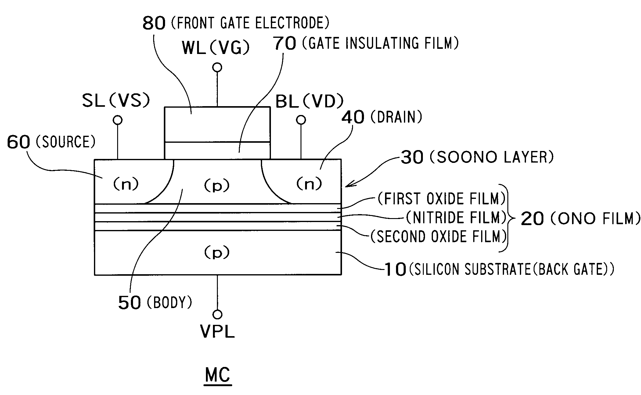
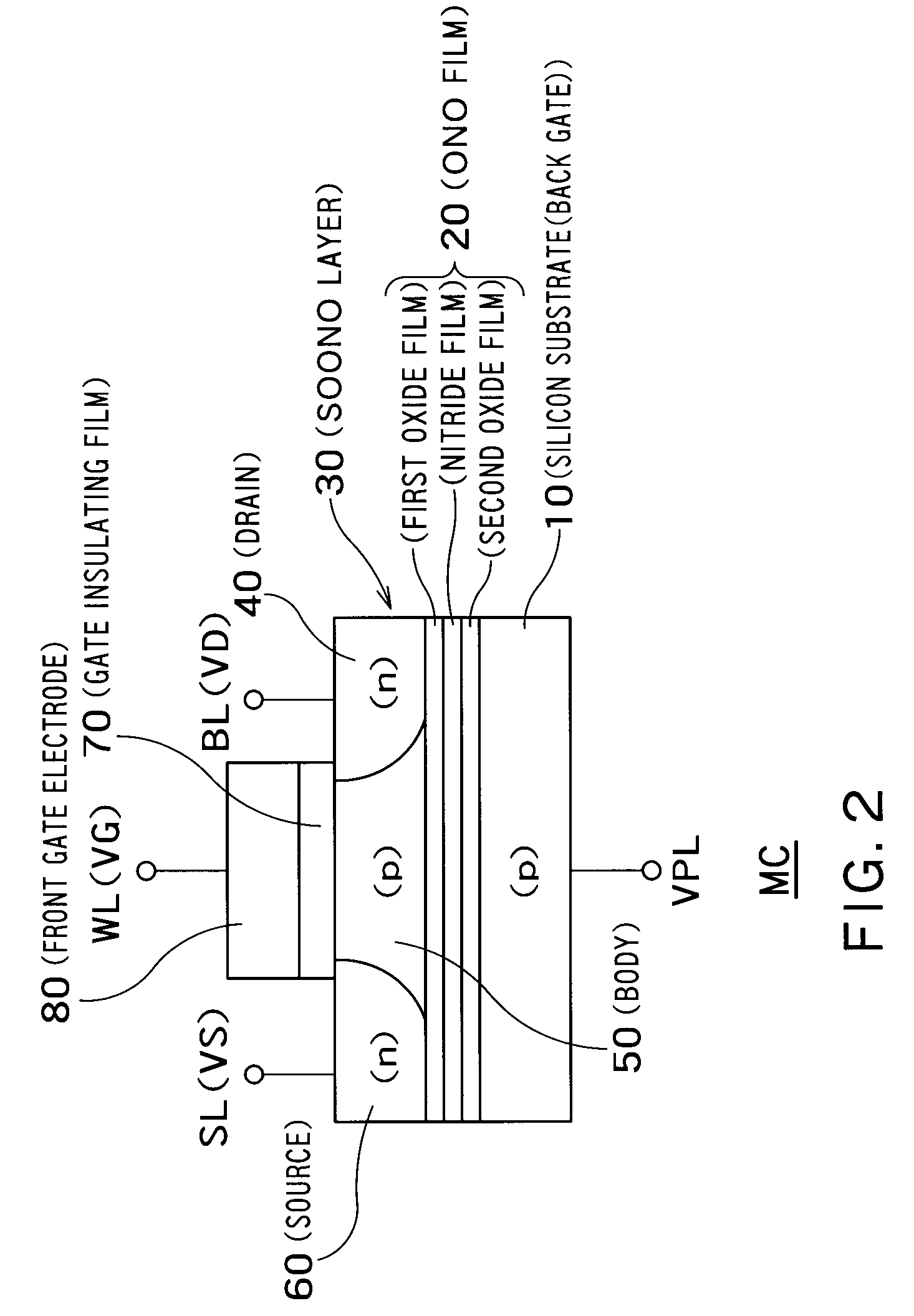
[0088]A memory cell according to a first embodiment of the present invention is configured by an MISFET formed on a silicon layer on a charge trapping film. A memory made up of such memory cells is a RAM which holds data dynamically depending on the number of majority carriers in the body region when a power supply is turned on. When the power supply is off, the RAM holds data depending on the amount of charges in the charge trapping film.

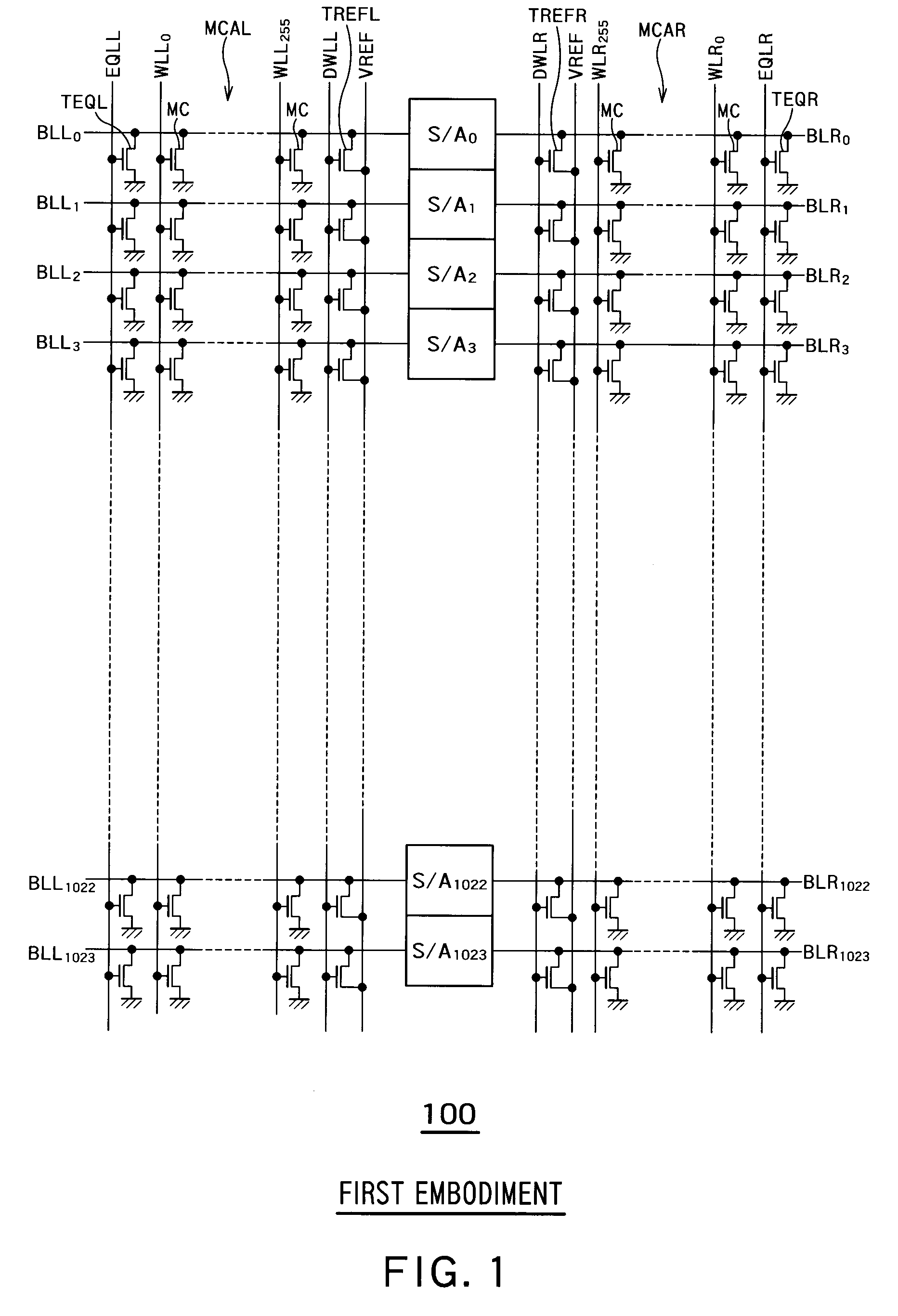
[0089]FIG. 1 is a schematic circuit diagram of an FBC memory device 100 according to the first embodiment. The FBC memory device 100 includes memory cells MC, word lines WLLi, WLRi (i is an integer) (also referred to as WL), bit lines BLLi, BLRi (also referred to as BL), sense amplifiers S / Ai (also referred to as S / A), dummy word lines DWLL, DWLR, reference potential lines VREF, reference transistors TREFL, TREFR, equalizing transistors TEQL, TEQR, and equalizing lines EQLL, EQLR.

[0090]The memory cells MC are arranged in a matrix to configure memor...

second embodiment

[0124]In a second embodiment of the present invention, an FBC memory device is shifted from the first storage state to the second storage state by the sequential save mode and from the second storage state to the first storage state by the sequential return mode. In the sequential save mode, a specific memory cell MC in the first storage state is selected by the word line WL and the bit line BL. The sense amplifier S / A reads the data stored in the memory cell MC (also referred to as selected memory cell MC). The sense amplifier S / A injects charges in the ONO film 20 based on the data. According to the sequential save mode, data is read from a selected memory cell MC in the first storage state. Data is programmed in the selected memory cell MC based on the read data. The memory cell MC is then shifted to the second storage state. These operations are performed sequentially upon all memory cells MC.

[0125]FIG. 10 is a flowchart of the sequential save mode and the sequential return mode...

third embodiment

Modified Example of Third Embodiment

[0180]FIG. 25 shows a memory cell array according to a modified example of the third embodiment. The modified example is different from the third embodiment in that the source line is driven selectively. FIG. 25 shows the voltage relationship when electrons are injected selectively in the ONO film 20 in the sequential save mode. In the modified example, a memory cell MC11 storing the data “1” and a memory cell MC 12 storing the data “0” are selected. A first voltage (e.g., 0 V) is applied to an unselected source line SL2. A second voltage which is higher than the first voltage (e.g., 1.7 V) is applied to a selected source line SL1. A third voltage which is lower than the first voltage (−1.7 V) is applied to unselected front word lines WL2 to WL4. A fourth voltage which is higher than the third voltage (e.g., 0.5 V) is applied to a selected front word line WL1. A fifth voltage which is higher than the fourth voltage (e.g., 3 V) is applied to the ba...


PUM


Abstract

This disclosure concerns a memory comprising a charge trapping film; a gate insulating film; a back gate on the charge trapping film; a front gate on the gate insulating film; and a body region provided between a drain and a source, wherein the memory includes a first storage state for storing data depending on the number of majority carriers in the body region and a second storage state for storing data depending on the amount of charges in the charge trapping film, and the memory is shifted from the first storage state to the second storage state by converting the number of majority carriers in the body region into the amount of charges in the charge trapping film or from the second storage state to the first storage state by converting the amount of charges in the charge trapping film into the number of majority carriers in the body region.

Description

CROSS-REFERENCE TO RELATED APPLICATION[0001]This application is based upon and claims the benefit of priority from the prior Japanese Patent Application No. 2006-268769, filed on Sep. 29, 2006, the entire contents of which are incorporated herein by reference.BACKGROUND OF THE INVENTION[0002]1. Field of the Invention[0003]The invention relates to a semiconductor memory device.[0004]2. Related Art[0005]FBC memory devices are semiconductor memory devices expected recently as alternatives to conventional DRAMs. In the FBC memory device, an FET (Field Effect Transistor) with a floating body (also referred to as body region) is formed on an SOI (Silicon On Insulator) substrate. Data “1” or “0” is stored depending on the number of majority carriers accumulated in the body region.[0006]Meanwhile, SOONO (Silicon-On-ONO) MOSFETs have been disclosed (C. W. Oh et. al., “A Novel Multi-Functional Silicon-On-ONO(SOONO) MOSFETs for SoC Applications: Electrical Characterization for High Performance...

Claims


Application Information

Patent Timeline
Patent Type & Authority Patents(United States)
IPC IPC(8): G11C14/00G11C16/04
CPCG11C11/404G11C14/0018H01L21/28282H01L29/792H01L27/11568H01L27/1203H01L29/42344H01L27/115G11C11/4074G11C2211/4016H01L29/785H01L29/78648H01L29/40117H10B43/30H10B69/00G11C11/406
Inventor SHINO, TOMOAKINITAYAMA, AKIHIROHAMAMOTO, TAKESHIAOCHI, HIDEAKIOHSAWA, TAKASHIFUKUDA, RYO
Owner TOSHIBA MEMORY CORP
Why Eureka
Try Eureka