Single spacer process for multiplying pitch by a factor greater than two and related intermediate IC structures

a single spacer and factor technology, applied in the field of single spacer process for multiplying pitch by a factor greater than two and related intermediate ic structures, can solve the problems of large processing cost, inability to reliably achieve the minimum pitch restriction of a given photolithographic technique, and large processing cos

Active Publication Date: 2009-11-03
MICRON TECH INC
View PDF157 Cites 608 Cited by
  • Summary
  • Abstract
  • Description
  • Claims
  • Application Information

AI Technical Summary

Problems solved by technology

However, due to factors such as optics and light (or radiation) wavelength, photolithography techniques each have a minimum pitch below which a particular photolithographic technique cannot reliably form features.
Consequently, the minimum pitch restriction of a given photolithographic technique is an impediment to further reduction in feature sizes.
Methods using multiple spacer formation steps for pitch multiplication lead to large processing costs.
Additionally, forming closely-spaced features entails use of high-resolution optical scanners, which can increase processing costs.
Additionally, photoresist materials currently available for use with 193 nm scanners are less robust than those available for 248 nm scanners, adding to the limitations of spacer formation on state-of-the-art photoresist masks.

Method used


Image

  • Single spacer process for multiplying pitch by a factor greater than two and related intermediate IC structures
  • Single spacer process for multiplying pitch by a factor greater than two and related intermediate IC structures
  • Single spacer process for multiplying pitch by a factor greater than two and related intermediate IC structures

Examples


Embodiment Construction

[0043]In accordance with embodiments of the invention, methods are provided in which pitch multiplication by a factor of 2n is accomplished using a single spacer step, thus providing substantial flexibility and savings in processing times and costs. Additionally, methods according to embodiments can be performed using less expensive optical scanners (e.g., 365 nm scanners), thus adding additional savings in processing costs.

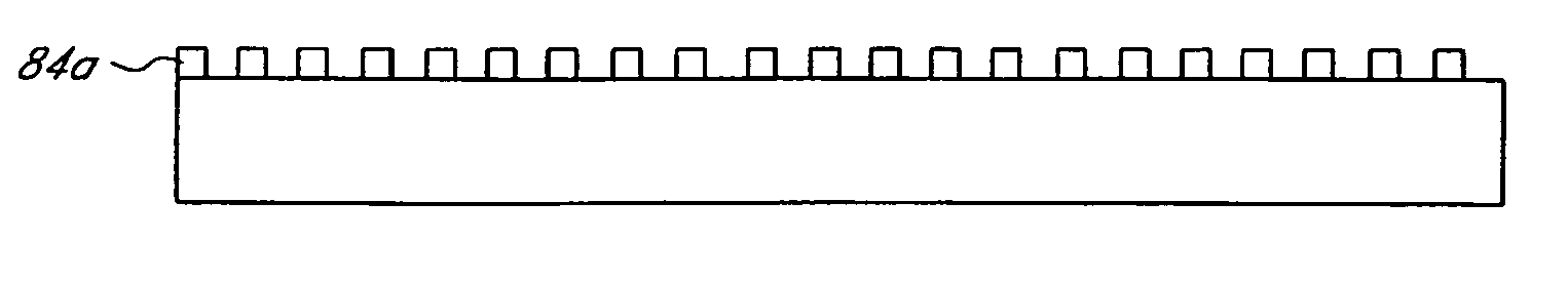
[0044]In accordance with embodiments of the invention, n, where n≧2, tiers of stacked mandrels are provided over a substrate. The substrate may comprise a silicon wafer, a wafer of another semiconductive material, or another bulk substrate including a layer of a semiconductive material, and one or more intervening layers, such as, e.g., hard mask layers. Each of the n tiers of mandrels can comprise a plurality of mandrels that are substantially parallel to one another. In one embodiment, the mandrels define parallel lines. Mandrels at tier n may be disposed over ...


PUM


Abstract

Single spacer processes for multiplying pitch by a factor greater than two are provided. In one embodiment, n, where n≧2, tiers of stacked mandrels are formed over a substrate, each of the n tiers comprising a plurality of mandrels substantially parallel to one another. Mandrels at tier n are over and parallel to mandrels at tier n−1, and the distance between adjoining mandrels at tier n is greater than the distance between adjoining mandrels at tier n−1. Spacers are simultaneously formed on sidewalls of the mandrels. Exposed portions of the mandrels are etched away and a pattern of lines defined by the spacers is transferred to the substrate.

Description

REFERENCE TO RELATED APPLICATIONS[0001]This application is related to and incorporates the following by reference in their entireties: U.S. patent application Ser. No. 11 / 150,408 of Wells, filed Jun. 9, 2005; U.S. patent application Ser. No. 11 / 144,543 of Sant et al., filed Jun. 2, 2005; and U.S. patent application Ser. No. 11 / 217,270 of Wells, filed Sep. 1, 2005; and U.S. patent application Ser. No. 11 / 134,982 of Abatchev et al., filed May 23, 2005.BACKGROUND OF THE INVENTION[0002]1. Field of the Invention[0003]This invention, in several embodiments, relates generally to masking techniques for semiconductor fabrication and, more particularly, to masking techniques including pitch multiplication.[0004]2. Description of the Related Art[0005]As a consequence of many factors, including demand for increased portability, computing power, memory capacity and energy efficiency, integrated circuits are continuously being reduced in size. The sizes of the constituent features that form the i...

Claims


Application Information

Patent Timeline
Patent Type & Authority Patents(United States)
IPC IPC(8): H01L21/44H01L21/311
CPCH01L21/0337H01L21/0338H01L21/3086H01L21/3088H01L21/31144H01L27/1052H01L23/5386H01L21/32139Y10S438/946Y10S438/947Y10S438/942H01L2924/0002H10B99/00H01L2924/00G03F7/70733
Inventor WELLS, DAVID H.ABATCHEV, MIRZAFER K.
Owner MICRON TECH INC
Why Eureka
Try Eureka