
Heterostructure self-assembled quantum dot

Inactive Publication Date: 2009-11-17
AIR FORCE US SEC THE
View PDF3 Cites 13 Cited by
  • Summary
  • Abstract
  • Description
  • Claims
  • Application Information

AI Technical Summary

Benefits of technology

[0008]A method and device for a heterostructure self-assembled quantum dot for the purpose of modification

Problems solved by technology

However, if the growth is immediately is rough and three-dimensional, the process is termed Volmer-Weber and no wetting layer is expected.
One of the major limitations of this type of quantum dot structure is that the confined region is composed of a single material.
This limitation restricts the tuning of the electron and hole wavefunctions and their associated properties.

Method used


Image

  • Heterostructure self-assembled quantum dot
  • Heterostructure self-assembled quantum dot
  • Heterostructure self-assembled quantum dot

Examples


Embodiment Construction

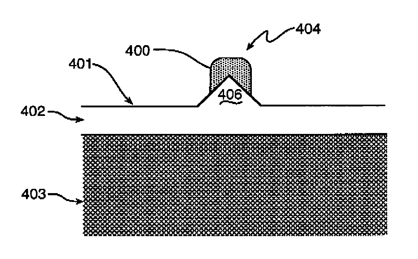
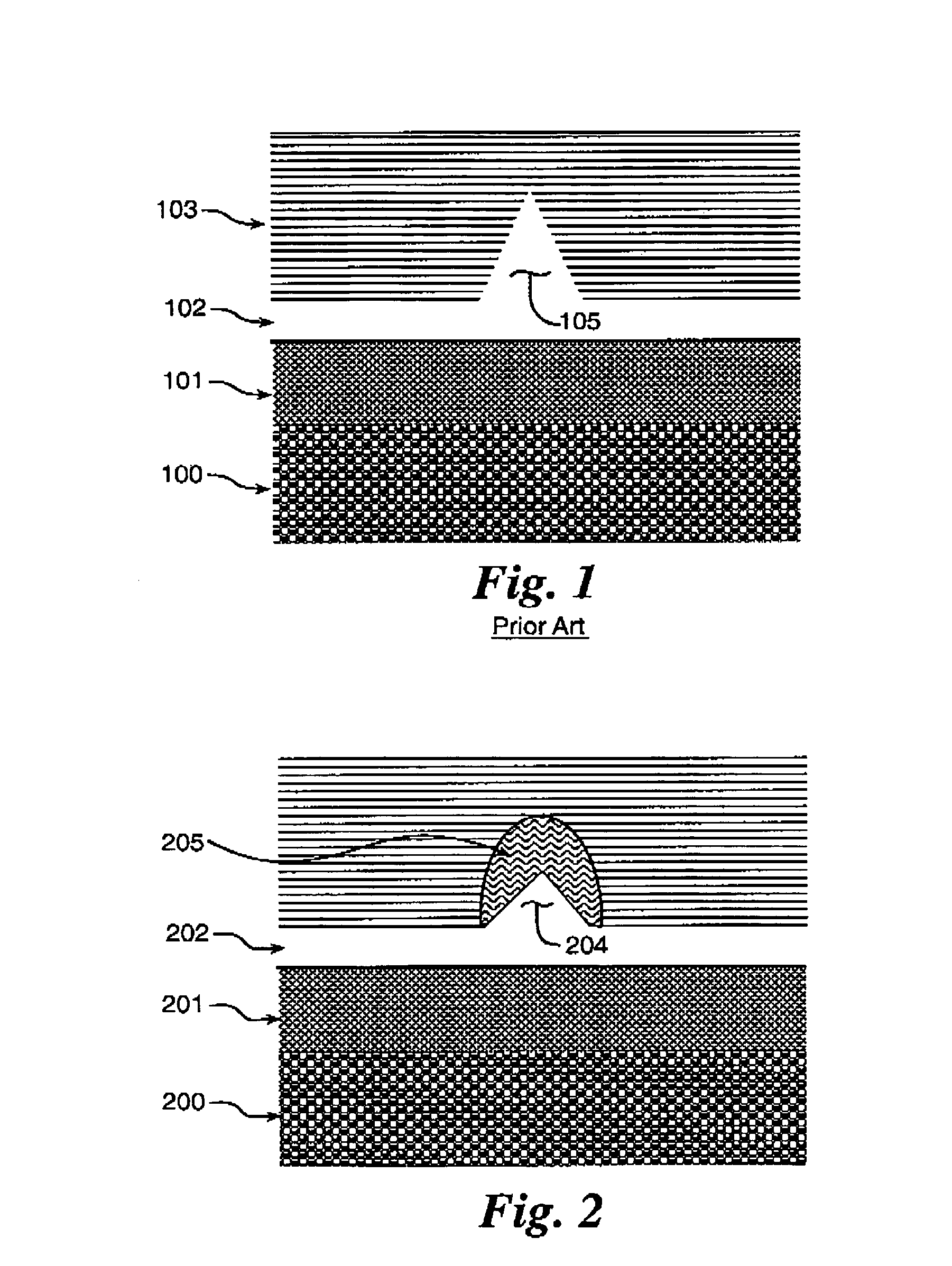
[0030]This present invention discloses and describes the formation of heterostructure self-assembled quantum dots (HeQuaDs) by utilizing the inherent strain profile present in an uncapped lattice mismatched quantum dot (such as in the case of InAs self-assembled quantum dots formed on GaAs, for example) to subsequently induce immediate hetero-epitaxy of a similarly strained material to form a composite dot structure as shown in FIG. 2. FIG. 2 shows a diagram of a heterojunction self-assembled quantum dot formed during epitaxial growth according to a preferred arrangement of the invention. After selecting a semiconductor substrate 200, materials are grown 201 that are nearly lattice matched on the substrate 200 using epitaxial growth techniques. This growth may be many layers depending on the application. Then a highly strained material 202 is deposited on the 201 surface to form a self-assembled quantum dot 204.

[0031]A similarly strained material is then deposited on the self-assemb...


PUM


Abstract

A method and device for a heterostructure self-assembled quantum dot based on inherent strain present in underlying self-assembled quantum dots for the purpose of modification and control of the properties of the self assembled quantum dots structures formed on semiconductor surfaces.

Description

RIGHTS OF THE GOVERNMENT[0001]The invention described herein may be manufactured and used by or for the Government of the United States for all governmental purposes without the payment of any royalty.BACKGROUND OF THE INVENTION[0002]Semiconductors have found wide use in a range of optical, electrical, and opto-electronic devices including amplifiers, detectors, and emitters. For the majority of these devices, high crystalline quality must be insured to prevent unwanted traps and scattering mechanisms. Typically these devices require the epitaxy of particular thicknesses of various semiconductors on one another. Initially, epitaxy was used to form bulk materials with different n and p doping in various regions. The advantage of introducing a different semiconductor, or other material, was realized and devices began to use heterojunctions to localize the electronic states and tailor their precise energy. A heterojunction occurs when dissimilar materials are brought together. This het...

Claims


Application Information

Patent Timeline
IPC IPC(8): H01L29/66
CPCH01L29/127B82Y10/00Y10S438/962
Inventor EYINK, KURT G.TOMICH, DAVID H.GRAZULIS, LAWRENCE
Owner AIR FORCE US SEC THE
Features
  • Generate Ideas
  • Intellectual Property
  • Life Sciences
  • Materials
  • Tech Scout
  • Unparalleled Data Quality
  • Higher Quality Content
  • 60% Fewer Hallucinations
Learn More