Wafer bonding hermetic encapsulation

a technology of adhesive bonding and hermetic encapsulation, which is applied in the direction of fluid speed measurement, semiconductor/solid-state device details, instruments, etc., can solve the problems of affecting the operation of the device, contaminating and failing the device, and the adhesive bond is subject to failure with time, and is especially prone to failur

Inactive Publication Date: 2009-11-24
INVENSAS BONDING TECH INC
View PDF14 Cites 67 Cited by
  • Summary
  • Abstract
  • Description
  • Claims
  • Application Information

AI Technical Summary

Benefits of technology

[0012]Another object of the present invention is to provide a method for encapsulation which does not require the fabrication of microheaters to produce localized heating.
[0023]Thus, in one aspect of the present invention, an encapsulated electronic or optoelectronic device, referred to as an (opto)electronic device, is produced having a device carrier including an (opto)electronic chip device and including a first bonding region encompassing the (opto)electronic chip device. The encapsulated (opto)electronic device includes an encapsulating member having a second bonding region. The encapsulating member is bonded to the device carrier along the first and second bonding regions by means of a non-adhesive direct contact bond. The encapsulating member provides a relief for the (opto)electronic chip device. Non-adhesive direct bonds are formed at low temperature (i.e. near room temperature) between the first and second bonding regions to encapsulate the (opto)electronic chip device.

Problems solved by technology

While effective in sealing the devices from the outside environment, the introduction of foreign materials into direct contact with the devices can impede operation of the devices and over time can contribute to the contamination and failure of the devices.
As a consequence, the adhesive bond is subject to failure with time and is especially prone to failure during heat cycles.
The complexity of the patterning and the operation of the micro-heaters add cost and are deterrents to the acceptance and utilization of microheaters.

Method used


Image

  • Wafer bonding hermetic encapsulation
  • Wafer bonding hermetic encapsulation
  • Wafer bonding hermetic encapsulation

Examples


examples

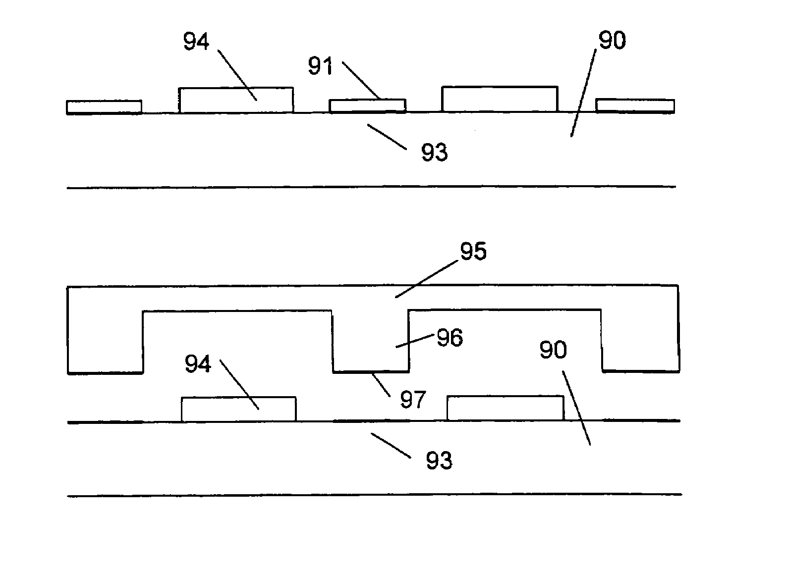
[0107]A concave MEMS device 71 is formed on a silicon device carrier 70 (FIG. 7A). Device carrier 70 has upper surface 72 surrounding each MEMS device 71; It is noted that the relative sizes of MEMS device 71 and the structure of carrier70 are not drawn to scale, but have been drawn merely to illustrate the principals of the invention. A removable photoresist layer 73 is formed over MEMS device 71, as shown in FIG. 7B. Layer 73 protects MEMS device 71 while not affecting the structure or operation of the MEMS device in any significant way after its removal. An example of layer 73 is photoresist. Subsequently, surface 72 is prepared for direct, non-adhesive room-temperature bonding by the method described above, namely, polishing to a surface roughness of preferably less than 0.5 nm followed by an activation process. The surface prepared for bonding is illustrated by the darker line 74 in FIG. 7C. Also shown in FIG. 7C is cover 75, which could also be a silicon layer having a lower s...


PUM


Abstract

A method for providing encapsulation of an electronic device which obtains an encapsulating member configured to enclose the electronic device, prepares a surface of the encapsulating member for non-adhesive direct bonding, prepares a surface of a device carrier including the electronic device for non-adhesive direct bonding, and bonds the prepared surface of the encapsulating member to the prepared surface of the device carrier to form an encapsulation of the electronic device. As such, an encapsulated electronic device results which includes the device carrier having a first bonding region encompassing the electronic device, includes the encapsulating member having at least one relief preventing contact between the electronic device and the encapsulating member and having a second bonding region bonded to the first bonding region of the device carrier, and includes a non-adhesive direct bond formed between the first and second bonding regions thereby to form an encapsulation of the electronic device. The encapsulated electronic device can be an electronic or optoelectronic device.

Description

CROSS-REFERENCE TO RELATED APPLICATIONS[0001]This application is related to U.S. patent application Method for Low Temperature Bonding and Bonded Structure, Ser. No. 09 / 505,283, filed Feb. 16, 2000, now U.S. Pat. No. 6,902,987, the entire contents of which are incorporated herein by reference, is related to U.S. patent application Three Dimensional Device Integration Method and Integrated Device, Ser. No. 09 / 410,054, filed Oct. 1, 1999, now U.S. Pat. No. 6,984,571, the entire contents of which are incorporated herein by reference, and is related to U.S. patent application Three Dimensional Device Integration Method and Integrated Device, Ser. No. 09 / 532,886, filed Mar. 22, 2000, now U.S. Pat. No. 6,500,694, the entire contents of which are incorporated herein by reference.BACKGROUND OF THE INVENTION[0002]1. Field of the Invention[0003]The invention is related to the packaging and encapsulation of semiconductor devices, including electronic devices, optoelectronic devices, microelect...

Claims


Application Information

Patent Timeline
Patent Type & Authority Patents(United States)
IPC IPC(8): H01L21/00B81B7/00H01L21/50H01L23/10
CPCB81C1/00269H01L21/50H01L23/10B81C2203/0118H01L2924/0002H01L2924/01079H01L2924/00
Inventor ENQUIST, PAUL M.TONG, QIN-YIFOUNTAIN, JR., GAIUS GILLMANMARKUNAS, ROBERT
Owner INVENSAS BONDING TECH INC
Why Eureka
Try Eureka