Non-volatile memory device and method of manufacturing the same

a memory device and non-volatile technology, applied in the direction of semiconductor devices, electrical devices, transistors, etc., can solve the problems of affecting reading disturbance between adjacent fins, and relatively high cost of soi substrates, so as to improve the effect of short channel effect and less susceptible

Inactive Publication Date: 2009-11-24
SAMSUNG ELECTRONICS CO LTD
View PDF11 Cites 221 Cited by
  • Summary
  • Abstract
  • Description
  • Claims
  • Application Information

AI Technical Summary

Benefits of technology

[0007]Example embodiments provide a non-volatile memory device less susceptible to reading disturbance and having an improved short channel effect.
[0008]Example embodiments also provide a method of manufacturing a non-volatile memory device less susceptible to reading disturbance and having an improved short channel effect.

Problems solved by technology

An SOI substrate may be relatively expensive.
Consequently, a reading disturbance may occur between adjacent fins.
Even when the SOI substrate is used, a short channel effect, e.g., a drain induced barrier lowering (DIBL), may cause problems depending on the dielectric characteristics of an insulator.

Method used


Image

  • Non-volatile memory device and method of manufacturing the same
  • Non-volatile memory device and method of manufacturing the same
  • Non-volatile memory device and method of manufacturing the same

Examples


Embodiment Construction

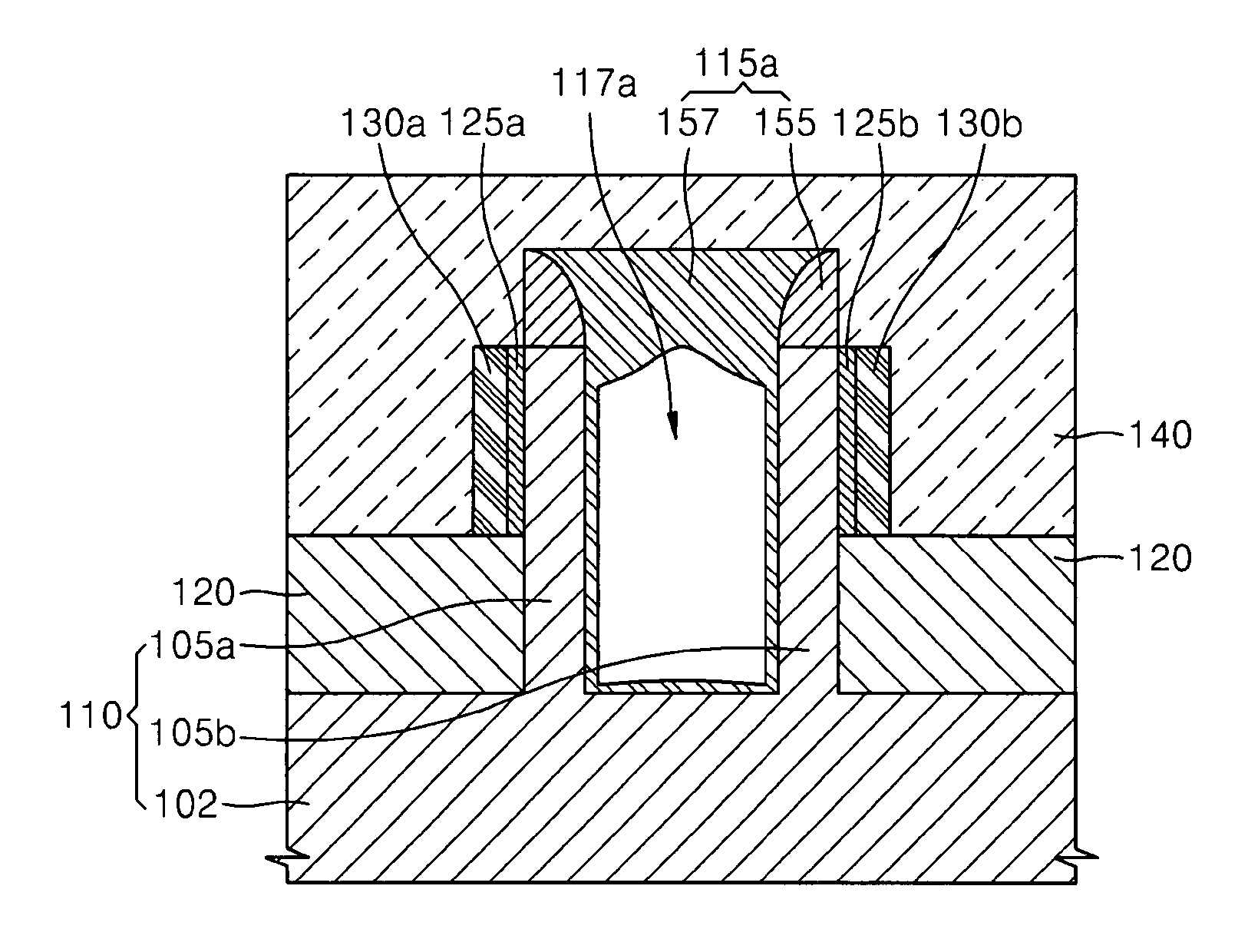
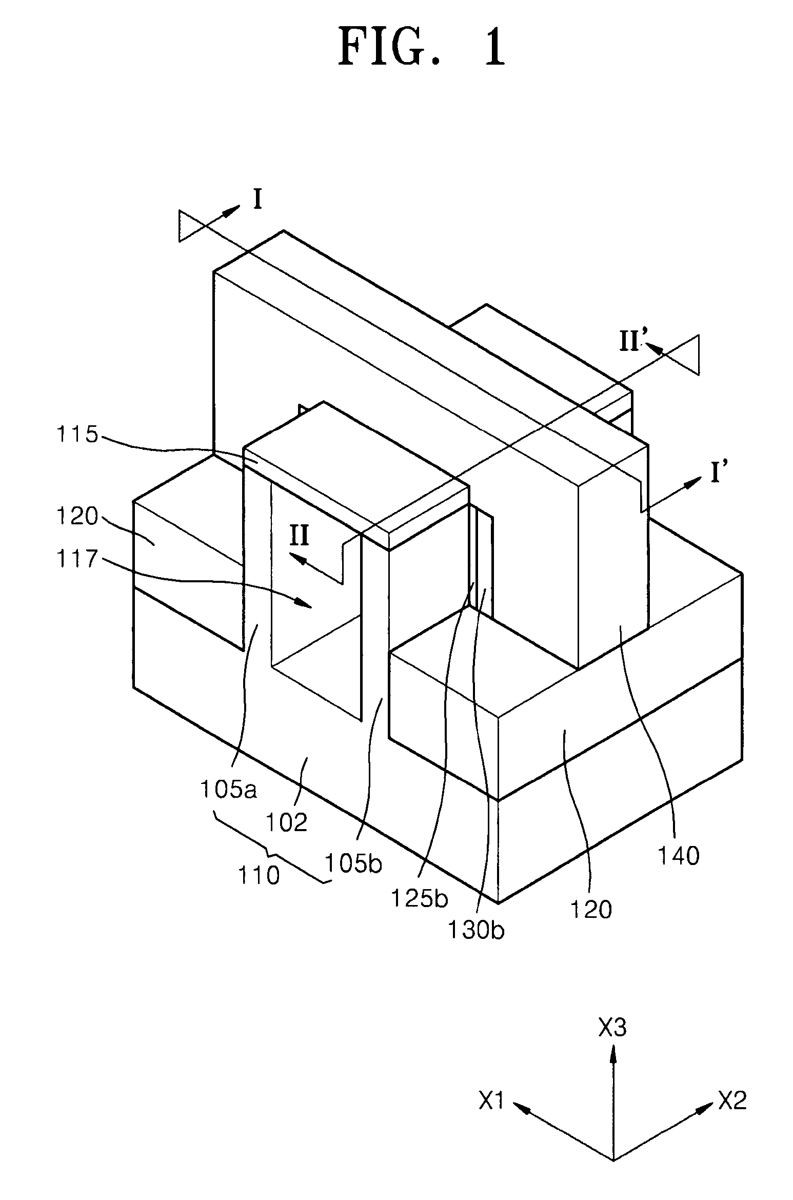
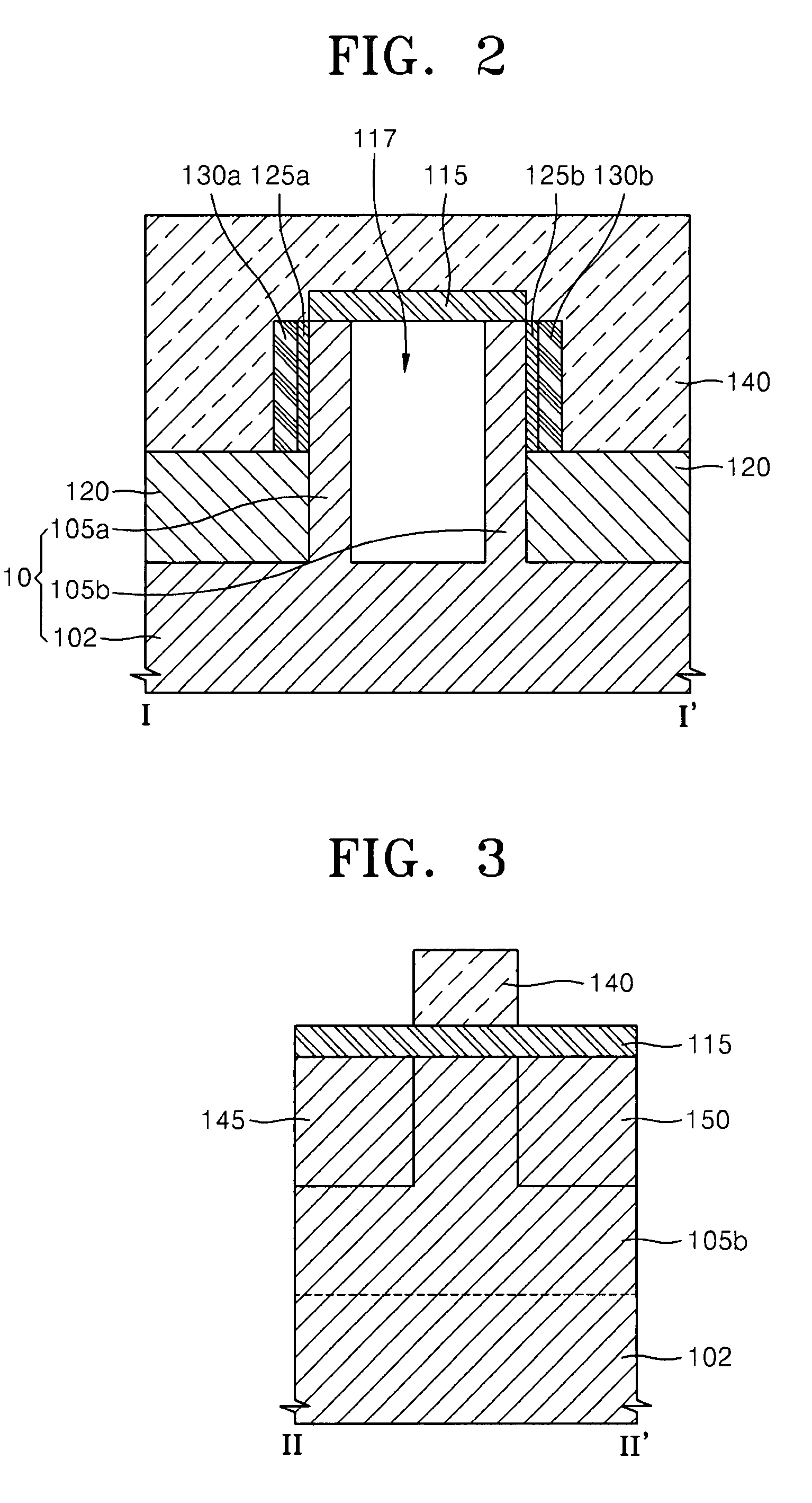
[0025]Example embodiments will now be described more fully with reference to the accompanying drawings, in which example embodiments are shown. Example embodiments may, however, be embodied in many different forms and should not be construed as being limited to the embodiments set forth herein; rather, these embodiments are provided so that this disclosure will be thorough and complete, and will fully convey the concept of example embodiments to those skilled in the art. In the drawings, the thicknesses of layers and regions are exaggerated for clarity.

[0026]It will be understood that when an element or layer is referred to as being “on,”“connected to”, “covering” or “coupled to” another element or layer, it can be directly on, connected, covering or coupled to the other element or layer or intervening elements or layers may be present. In contrast, when an element is referred to as being “directly on,”“directly connected to”, “directly covering” or “directly coupled to” another ele...


PUM


Abstract

The non-volatile memory device may include a semiconductor substrate having a body and a pair of fins. A bridge insulating layer may non-electrically connect upper portions of the pair of fins to define a void between the pair of fins. Outer surfaces of the pair of fins are the surfaces of the pair of fins that do not face the void and inner surfaces of the pair of fins are the surfaces of the pair of fins that do face the void. The non-volatile memory device may further include at least one control gate electrode that may cover at least a portion of outer surfaces of the pair of fins, may extend over the bridge insulating layer, and may be isolated from the semiconductor substrate. At least one pair of gate insulating layers may be between the at least one control gate electrode and the pair of fins, and at least one pair of storage nodes may be between the at least one pair of gate insulating layers and the at least one control gate electrode.

Description

PRIORITY STATEMENT[0001]This application claims priority under 35 USC §119 to Korean Patent Application Nos. 10-2006-0024903 and 10-2006-0113041, filed on Mar. 17, 2006 and Nov. 15, 2006 respectively, in the Korean Intellectual Property Office (KIPO), the entire contents of which are incorporated herein by reference.BACKGROUND[0002]1. Field[0003]Example embodiments relate to a non-volatile memory device and a method of manufacturing the same. Other example embodiments relate to a non-volatile memory device having a fin-type channel region and a method of manufacturing the same.[0004]2. Description of the Related Art[0005]As the dimensions of semiconductor products decrease, the volume of data that has to be processed by semiconductor products is increasing. A method of increasing the operating speed and integration of non-volatile memory devices used in semiconductor products has been studied. For example, in the case of a semiconductor device having an increased integration by usin...

Claims


Application Information

Patent Timeline
Patent Type & Authority Patents(United States)
IPC IPC(8): H01L29/76
CPCH01L21/764H01L27/115H01L27/11521H01L29/792H01L29/66825H01L29/66833H01L29/788H01L27/11568H10B69/00H10B41/30H10B43/30
Inventor PARK, YOON-DONGKIM, WON-JOOKOO, JUNE-MOKIM, SUK-PILHYUN, JAE-WOONGLEE, JUNG-HOON
Owner SAMSUNG ELECTRONICS CO LTD
Why Eureka
Try Eureka