Semiconductor device including multi-gate metal-insulator-semiconductor (MIS) transistor

a technology of metal-insulator-semiconductor and semiconductor device, which is applied in the direction of semiconductor device, basic electric element, electrical apparatus, etc., can solve the problems of device instability, unsuitable gaa-misfit polygonal channel, and breakdown of gate insulating film

Active Publication Date: 2009-11-24
KK TOSHIBA
View PDF18 Cites 41 Cited by
  • Summary
  • Abstract
  • Description
  • Claims
  • Application Information

AI Technical Summary

Problems solved by technology

The multi-gate MISFET as described above normally has a rectangular fin section, and therefore has the problem that electric field concentration readily occurs at corners, and this readily causes gate insulating film breakdown.
Accordingly, the polygonal channel formed by this method is unsuitable for a GAA-MISFET having the highest short channel effect immunity.
This is so because an electric field does not vertically symmetrically act, and this makes the device unstable.
Unfortunately, a dissimilar-material hetero-interface like this acts as a defect formation source and hence has an adverse effect on the reliability and leak characteristics of the device.
However, Ge greatly differs from Si in process conditions, and no process of forming a narrow fin by using Ge has been established yet.
Also, forming a GOI layer on an entire substrate having a large diameter makes the defect density very difficult to reduce.
A GOI substrate thus having many defects greatly increases the leakage current.

Method used


Image

  • Semiconductor device including multi-gate metal-insulator-semiconductor (MIS) transistor
  • Semiconductor device including multi-gate metal-insulator-semiconductor (MIS) transistor
  • Semiconductor device including multi-gate metal-insulator-semiconductor (MIS) transistor

Examples


first embodiment

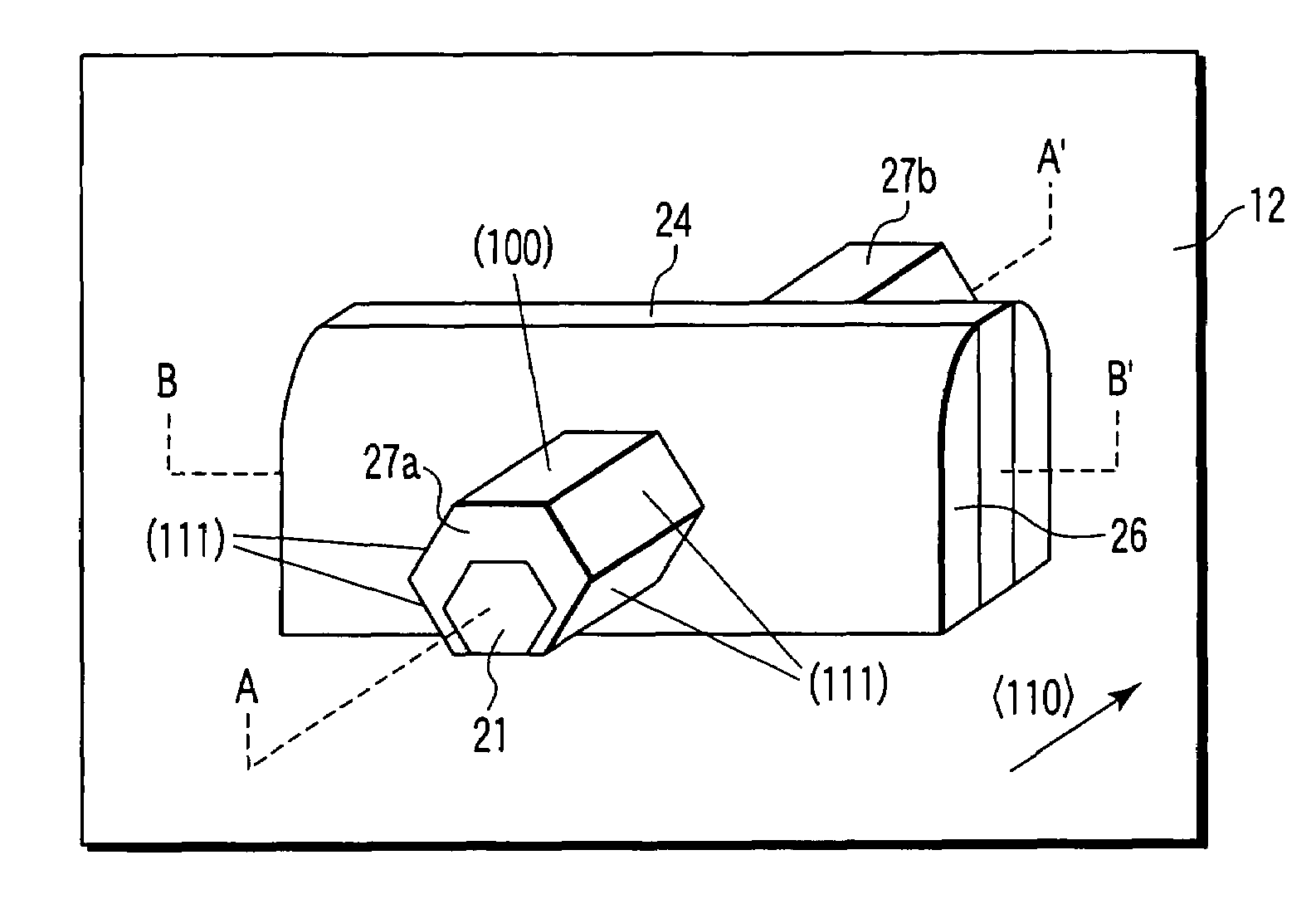
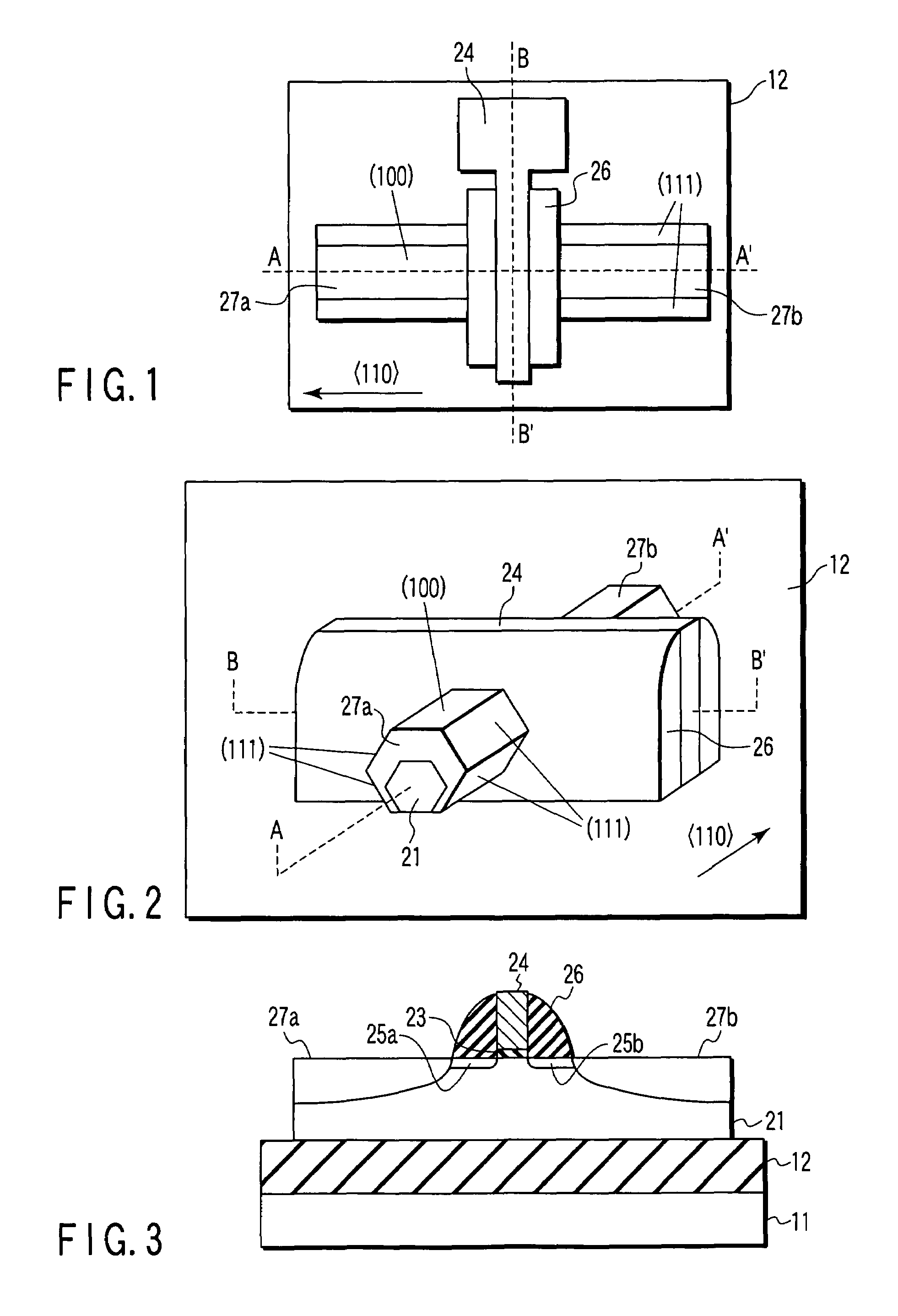
[0038]FIGS. 1 to 4 are views for explaining an outline of the arrangement of a multi-gate MISFET according to the first embodiment of the present invention. FIG. 1 is a plan view, FIG. 2 is a perspective view, FIG. 3 is a sectional view taken along a line A-A′ in FIG. 1, and FIG. 4 is a sectional view taken along a line B-B′ in FIG. 4.

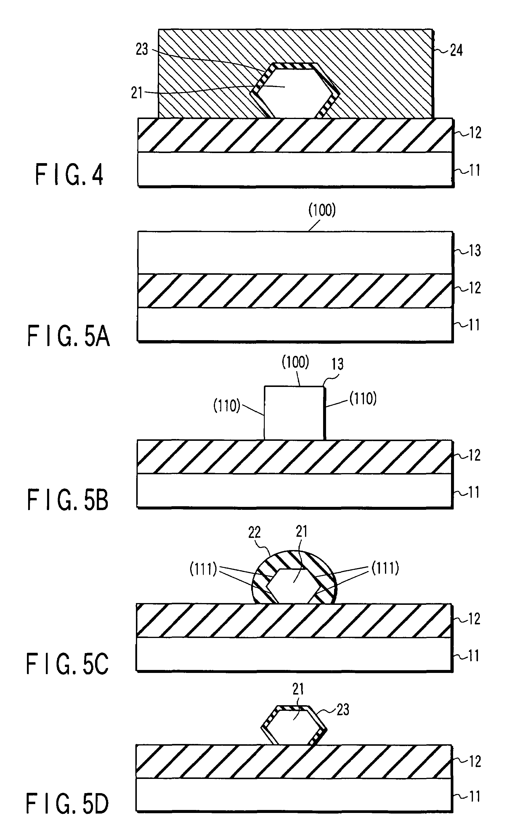
[0039]A buried insulating film 12 such as an Si oxide film is formed on a (100) Si substrate 11, and an island-like Ge layer (semiconductor layer) 21 is formed along the -axis direction on the buried insulating film 12 (FIGS. 1 to 4). The island (projection) of the Ge layer 21 is an active region for a FinFET. The Ge layer 21 has a hexagonal section perpendicular to the -axis direction, so all angles formed by adjacent side surfaces are larger than 90° (FIG. 2).

[0040]A gate insulating film 23 is formed on the side surfaces of the Ge layer 21 so as to surround the central portion of the Ge layer 21, and a gate electrode 24 is formed on the gate insulati...

second embodiment

[0064]FIGS. 12 to 14 are views for explaining an outline of the arrangement of a multi-gate MISFET according to the second embodiment of the present invention. FIG. 12 is a plan view, FIG. 13 is a sectional view taken along a line A-A′ in FIG. 12, and FIG. 14 is a sectional view taken along a line C-C′ in FIG. 12. Note that the same reference numerals as in FIGS. 1 to 4 denote the same parts, and a detailed explanation thereof will be omitted.

[0065]A channel made of a Ge layer 21, a gate insulating film 23, and a gate electrode 24 are the same as those of the first embodiment. This embodiment differs from the first embodiment in that Si or SiGe is epitaxially grown on extension regions as heavily doped regions which connect the channel and source / drain electrodes 27 and on the source / drain electrodes 27, thereby forming a so-called elevated extension structure.

[0066]That is, thin sidewall insulating films 31 are formed on the side surfaces of the gate electrode 24 and gate insulatin...


PUM


Abstract

In a semiconductor device including a multi-gate MIS transistor having a channel on a plurality of surfaces, a gate electrode is formed on a gate insulating film on side surfaces of an island-like semiconductor layer formed along a given direction on an insulating film, and source / drain electrodes are formed in contact with the semiconductor layer. The semiconductor layer has a plurality of side surfaces along the given direction. All angles formed by adjacent side surfaces are larger than 90°. A section perpendicular to the given direction is vertically and horizontally symmetrical.

Description

CROSS-REFERENCE TO RELATED APPLICATIONS[0001]This application is based upon and claims the benefit of priority from prior Japanese Patent Application No. 2006-038252, filed Feb. 15, 2006, the entire contents of which are incorporated herein by reference.BACKGROUND OF THE INVENTION[0002]1. Field of the Invention[0003]The present invention relates to a semiconductor device including a multi-gate metal-insulator-semiconductor (MIS) transistor having a channel on a plurality of surfaces, and a method of fabricating the same.[0004]2. Description of the Related Art[0005]Recently, a multi-gate MISFET having a strong short channel effect immunity is attracting attention. Examples of the multi-gate MISFET are a double-gate MISFET having gates on both the right and left surfaces of a projecting portion (fin) serving as an active region, a tri-gate MISFET having gates on three surfaces, i.e., the upper surface and the right and left surfaces, and a gate-all-around (GAA) MISFET in which a gate ...

Claims


Application Information

Patent Timeline
Patent Type & Authority Patents(United States)
IPC IPC(8): H01L27/12
CPCH01L29/78687H01L29/7853H01L29/66795H01L29/66636H01L21/18
Inventor IRISAWA, TOSHIFUMINUMATA, TOSHINORITAKAGI, SHINICHISUGIYAMA, NAOHARU
Owner KK TOSHIBA
Why Eureka
Try Eureka